
User guide


Table Of Contents
- Features
- Pin Configurations
- Overview
- AVR CPU Core
- AVR ATmega162 Memories
- System Clock and Clock Options
- Power Management and Sleep Modes
- System Control and Reset
- Interrupts
- I/O-Ports
- Introduction
- Ports as General Digital I/O
- Alternate Port Functions
- Register Description for I/O-Ports
- Port A Data Register – PORTA
- Port A Data Direction Register – DDRA
- Port A Input Pins Address – PINA
- Port B Data Register – PORTB
- Port B Data Direction Register – DDRB
- Port B Input Pins Address – PINB
- Port C Data Register – PORTC
- Port C Data Direction Register – DDRC
- Port C Input Pins Address – PINC
- Port D Data Register – PORTD
- Port D Data Direction Register – DDRD
- Port D Input Pins Address – PIND
- Port E Data Register – PORTE
- Port E Data Direction Register – DDRE
- Port E Input Pins Address – PINE
- External Interrupts
- 8-bit Timer/Counter0 with PWM
- Timer/Counter0, Timer/Counter1, and Timer/Counter3 Prescalers
- 16-bit Timer/Counter (Timer/Counter1 and Timer/Counter3)
- Restriction in ATmega161 Compatibility Mode
- Overview
- Accessing 16-bit Registers
- Timer/Counter Clock Sources
- Counter Unit
- Input Capture Unit
- Output Compare Units
- Compare Match Output Unit
- Modes of Operation
- Timer/Counter Timing Diagrams
- 16-bit Timer/Counter Register Description
- Timer/Counter1 Control Register A – TCCR1A
- Timer/Counter3 Control Register A – TCCR3A
- Timer/Counter1 Control Register B – TCCR1B
- Timer/Counter3 Control Register B – TCCR3B
- Timer/Counter1 – TCNT1H and TCNT1L
- Timer/Counter3 – TCNT3H and TCNT3L
- Output Compare Register 1 A – OCR1AH and OCR1AL
- Output Compare Register 1 B – OCR1BH and OCR1BL
- Output Compare Register 3 A – OCR3AH and OCR3AL
- Output Compare Register 3 B – OCR3BH and OCR3BL
- Input Capture Register 1 – ICR1H and ICR1L
- Input Capture Register 3 – ICR3H and ICR3L
- Timer/Counter Interrupt Mask Register – TIMSK(1)
- Extended Timer/Counter Interrupt Mask Register – ETIMSK(1)
- Timer/Counter Interrupt Flag Register – TIFR(1)
- Extended Timer/Counter Interrupt Flag Register – ETIFR(1)
- 8-bit Timer/Counter2 with PWM and Asynchronous operation
- Serial Peripheral Interface – SPI
- USART
- Analog Comparator
- JTAG Interface and On-chip Debug System
- IEEE 1149.1 (JTAG) Boundary-scan
- Boot Loader Support – Read-While-Write Self-programming
- Features
- Application and Boot Loader Flash Sections
- Read-While-Write and No Read-While-Write Flash Sections
- Boot Loader Lock Bits
- Entering the Boot Loader Program
- Addressing the Flash During Self- programming
- Self-programming the Flash
- Performing Page Erase by SPM
- Filling the Temporary Buffer (Page Loading)
- Performing a Page Write
- Using the SPM Interrupt
- Consideration while Updating BLS
- Prevent Reading the RWW Section During Self- programming
- Setting the Boot Loader Lock Bits by SPM
- EEPROM Write Prevents Writing to SPMCR
- Reading the Fuse and Lock Bits from Software
- Preventing Flash Corruption
- Programming Time for Flash When Using SPM
- Simple Assembly Code Example for a Boot Loader
- ATmega162 Boot Loader Parameters
- Memory Programming
- Program And Data Memory Lock Bits
- Fuse Bits
- Signature Bytes
- Calibration Byte
- Parallel Programming Parameters, Pin Mapping, and Commands
- Parallel Programming
- Enter Programming Mode
- Considerations for Efficient Programming
- Chip Erase
- Programming the Flash
- Programming the EEPROM
- Reading the Flash
- Reading the EEPROM
- Programming the Fuse Low Bits
- Programming the Fuse High Bits
- Programming the Extended Fuse Bits
- Programming the Lock Bits
- Reading the Fuse and Lock Bits
- Reading the Signature Bytes
- Reading the Calibration Byte
- Parallel Programming Characteristics
- Serial Downloading
- SPI Serial Programming Pin Mapping
- Programming via the JTAG Interface
- Programming Specific JTAG Instructions
- AVR_RESET (0xC)
- PROG_ENABLE (0x4)
- PROG_COMMANDS (0x5)
- PROG_PAGELOAD (0x6)
- PROG_PAGEREAD (0x7)
- Data Registers
- Reset Register
- Programming Enable Register
- Programming Command Register
- Virtual Flash Page Load Register
- Virtual Flash Page Read Register
- Programming Algorithm
- Entering Programming Mode
- Leaving Programming Mode
- Performing Chip Erase
- Programming the Flash
- Reading the Flash
- Programming the EEPROM
- Reading the EEPROM
- Programming the Fuses
- Programming the Lock Bits
- Reading the Fuses and Lock Bits
- Reading the Signature Bytes
- Reading the Calibration Byte
- Electrical Characteristics
- ATmega162 Typical Characteristics
- Active Supply Current
- Idle Supply Current
- Power-down Supply Current
- Power-save Supply Current
- Standby Supply Current
- Pin Pull-up
- Pin Driver Strength
- Pin Thresholds and Hysteresis
- BOD Thresholds and Analog Comparator Offset
- Internal Oscillator Speed
- Current Consumption of Peripheral Units
- Current Consumption in Reset and Reset Pulsewidth
- Register Summary
- Instruction Set Summary
- Ordering Information
- Packaging Information
- Erratas
- Datasheet Change Log for ATmega162
- Table of Contents
12
ATmega162/V
2513E–AVR–09/03
Instruction Execution
Timing
This section describes the general access timing concepts for instruction execution. The
AVR CPU is driven by the CPU clock clk
CPU
, directly generated from the selected clock
source for the chip. No internal clock division is used.
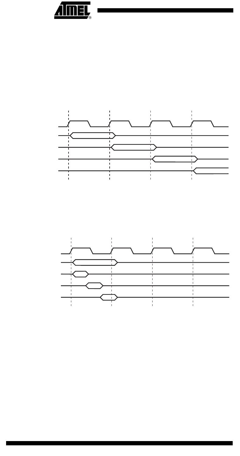
Figure 6 shows the parallel instruction fetches and instruction executions enabled by the
Harvard architecture and the fast-access Register File concept. This is the basic pipelin-
ing concept to obtain up to 1 MIPS per MHz with the corresponding unique results for
functions per cost, functions per clocks, and functions per power-unit.
Figure 6. The Parallel Instruction Fetches and Instruction Executions
Figure 7 shows the internal timing concept for the Register File. In a single clock cycle
an ALU operation using two register operands is executed, and the result is stored back
to the destination register.
Figure 7. Single Cycle ALU Operation
Reset and Interrupt
Handling
The AVR provides several different interrupt sources. These interrupts and the separate
Reset Vector each have a separate program vector in the program memory space. All
interrupts are assigned individual enable bits which must be written logic one together
with the Global Interrupt Enable bit in the Status Register in order to enable the interrupt.
Depending on the Program Counter value, interrupts may be automatically disabled
when Boot Lock bits BLB02 or BLB12 are programmed. This feature improves software
security. See the section “Memory Programming” on page 230 for details.
The lowest addresses in the program memory space are by default defined as the Reset
and Interrupt Vectors. The complete list of vectors is shown in “Interrupts” on page 56.
The list also determines the priority levels of the different interrupts. The lower the
address the higher is the priority level. RESET has the highest priority, and next is INT0
– the External Interrupt Request 0. The Interrupt Vectors can be moved to the start of
the Boot Flash section by setting the IVSEL bit in the General Interrupt Control Register
(GICR). Refer to “Interrupts” on page 56 for more information. The Reset Vector can
clk
1st Instruction Fetch
1st Instruction Execute
2nd Instruction Fetch
2nd Instruction Execute
3rd Instruction Fetch
3rd Instruction Execute
4th Instruction Fetch
T1 T2 T3 T4
CPU
Total Execution Time
Register Operands Fetch
ALU Operation Execute
Result Write Back
T1 T2 T3 T4
clk
CPU