
User guide


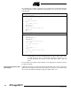
Table Of Contents
- Features
- Pin Configurations
- Overview
- AVR CPU Core
- AVR ATmega162 Memories
- System Clock and Clock Options
- Power Management and Sleep Modes
- System Control and Reset
- Interrupts
- I/O-Ports
- Introduction
- Ports as General Digital I/O
- Alternate Port Functions
- Register Description for I/O-Ports
- Port A Data Register – PORTA
- Port A Data Direction Register – DDRA
- Port A Input Pins Address – PINA
- Port B Data Register – PORTB
- Port B Data Direction Register – DDRB
- Port B Input Pins Address – PINB
- Port C Data Register – PORTC
- Port C Data Direction Register – DDRC
- Port C Input Pins Address – PINC
- Port D Data Register – PORTD
- Port D Data Direction Register – DDRD
- Port D Input Pins Address – PIND
- Port E Data Register – PORTE
- Port E Data Direction Register – DDRE
- Port E Input Pins Address – PINE
- External Interrupts
- 8-bit Timer/Counter0 with PWM
- Timer/Counter0, Timer/Counter1, and Timer/Counter3 Prescalers
- 16-bit Timer/Counter (Timer/Counter1 and Timer/Counter3)
- Restriction in ATmega161 Compatibility Mode
- Overview
- Accessing 16-bit Registers
- Timer/Counter Clock Sources
- Counter Unit
- Input Capture Unit
- Output Compare Units
- Compare Match Output Unit
- Modes of Operation
- Timer/Counter Timing Diagrams
- 16-bit Timer/Counter Register Description
- Timer/Counter1 Control Register A – TCCR1A
- Timer/Counter3 Control Register A – TCCR3A
- Timer/Counter1 Control Register B – TCCR1B
- Timer/Counter3 Control Register B – TCCR3B
- Timer/Counter1 – TCNT1H and TCNT1L
- Timer/Counter3 – TCNT3H and TCNT3L
- Output Compare Register 1 A – OCR1AH and OCR1AL
- Output Compare Register 1 B – OCR1BH and OCR1BL
- Output Compare Register 3 A – OCR3AH and OCR3AL
- Output Compare Register 3 B – OCR3BH and OCR3BL
- Input Capture Register 1 – ICR1H and ICR1L
- Input Capture Register 3 – ICR3H and ICR3L
- Timer/Counter Interrupt Mask Register – TIMSK(1)
- Extended Timer/Counter Interrupt Mask Register – ETIMSK(1)
- Timer/Counter Interrupt Flag Register – TIFR(1)
- Extended Timer/Counter Interrupt Flag Register – ETIFR(1)
- 8-bit Timer/Counter2 with PWM and Asynchronous operation
- Serial Peripheral Interface – SPI
- USART
- Analog Comparator
- JTAG Interface and On-chip Debug System
- IEEE 1149.1 (JTAG) Boundary-scan
- Boot Loader Support – Read-While-Write Self-programming
- Features
- Application and Boot Loader Flash Sections
- Read-While-Write and No Read-While-Write Flash Sections
- Boot Loader Lock Bits
- Entering the Boot Loader Program
- Addressing the Flash During Self- programming
- Self-programming the Flash
- Performing Page Erase by SPM
- Filling the Temporary Buffer (Page Loading)
- Performing a Page Write
- Using the SPM Interrupt
- Consideration while Updating BLS
- Prevent Reading the RWW Section During Self- programming
- Setting the Boot Loader Lock Bits by SPM
- EEPROM Write Prevents Writing to SPMCR
- Reading the Fuse and Lock Bits from Software
- Preventing Flash Corruption
- Programming Time for Flash When Using SPM
- Simple Assembly Code Example for a Boot Loader
- ATmega162 Boot Loader Parameters
- Memory Programming
- Program And Data Memory Lock Bits
- Fuse Bits
- Signature Bytes
- Calibration Byte
- Parallel Programming Parameters, Pin Mapping, and Commands
- Parallel Programming
- Enter Programming Mode
- Considerations for Efficient Programming
- Chip Erase
- Programming the Flash
- Programming the EEPROM
- Reading the Flash
- Reading the EEPROM
- Programming the Fuse Low Bits
- Programming the Fuse High Bits
- Programming the Extended Fuse Bits
- Programming the Lock Bits
- Reading the Fuse and Lock Bits
- Reading the Signature Bytes
- Reading the Calibration Byte
- Parallel Programming Characteristics
- Serial Downloading
- SPI Serial Programming Pin Mapping
- Programming via the JTAG Interface
- Programming Specific JTAG Instructions
- AVR_RESET (0xC)
- PROG_ENABLE (0x4)
- PROG_COMMANDS (0x5)
- PROG_PAGELOAD (0x6)
- PROG_PAGEREAD (0x7)
- Data Registers
- Reset Register
- Programming Enable Register
- Programming Command Register
- Virtual Flash Page Load Register
- Virtual Flash Page Read Register
- Programming Algorithm
- Entering Programming Mode
- Leaving Programming Mode
- Performing Chip Erase
- Programming the Flash
- Reading the Flash
- Programming the EEPROM
- Reading the EEPROM
- Programming the Fuses
- Programming the Lock Bits
- Reading the Fuses and Lock Bits
- Reading the Signature Bytes
- Reading the Calibration Byte
- Electrical Characteristics
- ATmega162 Typical Characteristics
- Active Supply Current
- Idle Supply Current
- Power-down Supply Current
- Power-save Supply Current
- Standby Supply Current
- Pin Pull-up
- Pin Driver Strength
- Pin Thresholds and Hysteresis
- BOD Thresholds and Analog Comparator Offset
- Internal Oscillator Speed
- Current Consumption of Peripheral Units
- Current Consumption in Reset and Reset Pulsewidth
- Register Summary
- Instruction Set Summary
- Ordering Information
- Packaging Information
- Erratas
- Datasheet Change Log for ATmega162
- Table of Contents

103
ATmega162/V
2513E–AVR–09/03
Timer/Counter0,
Timer/Counter1, and
Timer/Counter3
Prescalers
Timer/Counter3, Timer/Counter1, and Timer/Counter0 share the same prescaler mod-
ule, but the Timer/Counters can have different prescaler settings. The description below
applies to Timer/Counter3, Timer/Counter1, and Timer/Counter0.
Internal Clock Source The Timer/Counter can be clocked directly by the system clock (by setting the CSn2:0 =
1). This provides the fastest operation, with a maximum Timer/Counter clock frequency
equal to system clock frequency (f
CLK_I/O
). Alternatively, one of four taps from the pres-
caler can be used as a clock source. The prescaled clock has a frequency of either
f
CLK_I/O
/8, f
CLK_I/O
/64, f
CLK_I/O
/256, or f
CLK_I/O
/1024. In addition, Timer/Counter3 has the
option of choosing f
CLK_I/O
/16 and f
CLK_I/O
/32.
Prescaler Reset The prescaler is free running, i.e., operates independently of the clock select logic of the
Timer/Counter, and it is shared by Timer/Counter3, Timer/Counter1, and
Timer/Counter0. Since the prescaler is not affected by the Timer/Counter’s clock select,
the state of the prescaler will have implications for situations where a prescaled clock is
used. One example of prescaling artifacts occurs when the Timer is enabled and
clocked by the prescaler (6 > CSn2:0 > 1). The number of system clock cycles from
when the Timer is enabled to the first count occurs can be from 1 to N+1 system clock
cycles, where N equals the prescaler divisor (8, 64, 256, or 1024, additional selections
for Timer/Counter3: 32 and 64).
It is possible to use the Prescaler Reset for synchronizing the Timer/Counter to program
execution. However, care must be taken if the other Timer/Counter that shares the
same prescaler also uses prescaling. A Prescaler Reset will affect the prescaler period
for all Timer/Counters it is connected to.
External Clock Source An external clock source applied to the Tn/T0 pin can be used as Timer/Counter clock
(clk
T1
/clk
T
0) for Timer/Counter1 and Timer/Counter0. The Tn/T0 pin is sampled once
every system clock cycle by the pin synchronization logic. The synchronized (sampled)
signal is then passed through the edge detector. Figure 44 shows a functional equiva-
lent block diagram of the Tn/T0 synchronization and edge detector logic. The registers
are clocked at the positive edge of the internal system clock (
clk
I/O
). The latch is trans-
parent in the high period of the internal system clock.
The edge detector generates one clk
T1
/clk
T
0
pulse for each positive (CSn2:0 = 7) or neg-
ative (CSn2:0 = 6) edge it detects.
Figure 44. Tn/T0 Pin Sampling
The synchronization and edge detector logic introduces a delay of 2.5 to 3.5 system
clock cycles from an edge has been applied to the Tn/T0 pin to the counter is updated.
Enabling and disabling of the clock input must be done when Tn/T0 has been stable for
at least one system clock cycle, otherwise it is a risk that a false Timer/Counter clock
pulse is generated.
Tn_sync
(To Clock
Select Logic)
Edge DetectorSynchronization
DQDQ
LE
DQ
Tn
clk
I/O