ATmega128RFA1 Features ® • High Performance, Low Power AVR 8-Bit Microcontroller • Advanced RISC Architecture - 135 Powerful Instructions – Most Single Clock Cycle Execution - 32x8 General Purpose Working Registers - Fully Static Operation - Up to 16 MIPS Throughput at 16 MHz and 1.
1 Pin Configurations [PE3:OC3A:AIN1] [PE4:OC3B:INT4] [PE5:OC3C:INT5] [PE6:T3:INT6] [PE7:ICP3:INT7:CLKO] [DEVDD] [DVSS] [XTAL2] [AVSS] [XTAL1] [EVDD] [AVDD] [AVSS:ASVSS] [AREF] [PF0:ADC0] [PF1:ADC1] Figure 1-1.
ATmega128RFA1 3 Overview The ATmega128RFA1 is a low-power CMOS 8 bit microcontroller based on the AVR enhanced RISC architecture combined with a high data rate transceiver for the 2.4 GHz ISM band. It is derived from the ATmega1281 microcontroller and the AT86RF231 radio transceiver. By executing powerful instructions in a single clock cycle, the device achieves throughputs approaching 1 MIPS per MHz allowing the system designer to optimize power consumption versus processing speed.
Spectrum Signal (DSSS) processing with spreading and despreading. The device is fully compatible with IEEE802.15.4-2006/2003 and ZigBee standards.
ATmega128RFA1 trough an SPI serial interface, by a conventional nonvolatile memory programmer, or by on on-chip boot program running on the AVR core. The boot program can use any interface to download the application program in the application Flash memory. Software in the boot Flash section will continue to run while the application Flash section is updated, providing true Read-While-Write operation.
3.2.10 Port F (PF7...PF0) Port F is an 8-bit bi-directional I/O port with internal pull-up resistors (selected for each bit). The Port F output buffers have symmetrical drive characteristics with both high sink and source capability. As inputs, Port F pins that are externally pulled low will source current if the pull-up resistors are activated. The Port F pins are tri-stated when a reset condition becomes active, even if the clock is not running.
ATmega128RFA1 registers are unchanged as long as it fits the target application of a very small and power efficient radio system. In addition, several new features were added. Backward compatibility of the ATmega128RFA1 to the ATmega1281/2561 is provided in most cases. However some incompatibilities between the microcontrollers exist. 3.3.1 Port A and Port C Port A and Port C are not implemented. The associated registers are available but will not provide any port control.
• over 10 years at 85°C • TBD years at 25°C.
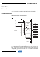
ATmega128RFA1 7 AVR CPU Core 7.1 Introduction This section discusses the AVR core architecture in general. The main function of the CPU core is to ensure correct program execution. The CPU must therefore be able to access memories, perform calculation, control peripherals, and handle interrupts. 7.2 Architectural Overview Figure 7-1.
The fast-access Register File contains 32 x 8-bit general purpose working registers with a single clock cycle access time. This allows single-cycle Arithmetic Logic Unit (ALU) operation. In a typical ALU operation, two operands are output from the Register File, the operation is executed, and the result is stored back in the Register File – in one clock cycle.
ATmega128RFA1 7.4 Status Register The Status Register contains information about the result of the most recently executed arithmetic instruction. This information can be used for altering program flow in order to perform conditional operations. Note that the Status Register is updated after all ALU operations, as specified in the Instruction Set Reference. This will in many cases remove the need for using the dedicated compare instructions, resulting in faster and more compact code.
stored when entering an interrupt routine and restored when returning from an interrupt routine. This must be handled by software. 7.5 General Purpose Register File The Register File is optimized for the AVR Enhanced RISC instruction set.
ATmega128RFA1 Figure 7-2. The X-, Y-, Z-registers In the different addressing modes these address registers have functions as fixed displacement, automatic increment, and automatic decrement (see the instruction set reference for details). 7.6 Stack Pointer The Stack is mainly used for storing temporary data, for storing local variables and for storing return addresses after interrupts and subroutine calls. The Stack Pointer Register always points to the top of the Stack.
7.6.2 SPL – Stack Pointer Low Bit 7 6 5 4 3 2 1 0 $3D ($5D) SP7 SP6 SP5 SP4 SP3 SP2 SP1 SP0 Read/Write Initial Value RW 1 RW 1 RW 1 RW 1 RW 1 RW 1 RW 1 RW 1 SPL The AVR Stack Pointer is implemented as two 8-bit registers SPL and SPH in the I/O space. The number of bits actually used is implementation dependent. Note that the data space in some implementations of the AVR architecture is so small that only SPL is needed. In this case, the SPH Register will not be present.
ATmega128RFA1 7.7 Instruction Execution Timing Figure 7-4. The Parallel Instruction Fetches and Instruction Executions T1 T2 T3 T4 clkCPU 1st Instruction Fetch 1st Instruction Execute 2nd Instruction Fetch 2nd Instruction Execute 3rd Instruction Fetch 3rd Instruction Execute 4th Instruction Fetch Figure 7-5 below shows the internal timing concept for the Register File.
interrupts. All enabled interrupts can then interrupt the current interrupt routine. The I-bit is automatically set when a Return from Interrupt instruction – RETI – is executed. There are basically two types of interrupts. The first type is triggered by an event that sets the Interrupt Flag. For these interrupts, the Program Counter is vectored to the actual Interrupt Vector in order to execute the interrupt handling routine, and hardware clears the corresponding Interrupt Flag.
ATmega128RFA1 Assembly Code Example ; note: will enter sleep before any pending ; interrupt(s) C Code Example __enable_interrupt(); /* set Global Interrupt Enable */ __sleep(); /* enter sleep, waiting for interrupt */ /* note: will enter sleep before any pending interrupt(s) */ 7.8.1 Interrupt Response Time The interrupt execution response for all the enabled AVR interrupts is five clock cycles minimum.
8 AVR Memories This section describes the different memories in the ATmega128RFA1. The AVR architecture has two main memory spaces, the Data Memory and the Program Memory space. In addition, the ATmega128RFA1 features an EEPROM Memory for data storage. All three memory spaces are linear and regular. 8.1 In-System Reprogrammable Flash Program Memory The ATmega128RFA1 contains 128K bytes On-chip In-System Reprogrammable Flash memory for program storage, see Figure 8-6 below.
ATmega128RFA1 The five different addressing modes for the data memory cover: Direct, Indirect with Displacement, Indirect, Indirect with Pre-decrement, and Indirect with Post-increment. In the Register file, registers R26 to R31 feature the indirect addressing pointer registers. The direct addressing reaches the entire data space. The Indirect with Displacement mode reaches 63 address locations from the base address given by the Y- or Z-register.
Figure 8-8. On-Chip Data SRAM Access Cycles T1 T2 T3 clkCPU Address Compute Address Address valid Write Data WR Read Data RD Memory Access Instruction Next Instruction 8.3 EEPROM Data Memory The ATmega128RFA1 contains 4Kbyte of data EEPROM memory. It is organized as a separate data space, in which single bytes can be read and written. The EEPROM has an endurance of at least 2000 write/erase cycles.
ATmega128RFA1 The following code examples show one assembly and one C function for writing to the EEPROM. The examples assume that interrupts are controlled (e.g. by disabling interrupts globally) so that no interrupts will occur during execution of these functions. The examples also assume that no Flash Boot Loader is present in the software. If such code is present, the EEPROM write function must also wait for any ongoing SPM command to finish.
Assembly Code Example sbic EECR,EEPE rjcmp EEPROM_read ; Set up address (r18:r17) in address register out EEARH, r18 out EEARL, r17 ; Start eeprom read by writing EERE sbi EECR,EERE ; Read data from Data Register in r16,EEDR ret C Code Example unsigned char EEPROM_read(unsigned int uiAddress) { /* Wait for completion of previous write */ while(EECR & (1<
ATmega128RFA1 8.4 EEPROM Register Description 8.4.1 EEARH – EEPROM Address Register High Byte Bit $22 ($42) Read/Write Initial Value 7 6 5 4 Res3 Res2 Res1 Res0 R 0 R 0 R 0 R 0 3 2 EEAR11 EEAR10 RW X RW X 1 0 EEAR9 EEAR8 RW X RW X EEARH The EEPROM Address Registers EEARH and EEARL specify the EEPROM address in the 4K bytes EEPROM space. The EEPROM data bytes are addressed linearly between 0 and 4096. The initial value of EEAR is undefined.
8.4.4 EECR – EEPROM Control Register Bit $1F ($3F) 7 6 5 4 3 2 1 0 Res1 Res0 EEPM1 EEPM0 EERIE EEMPE EEPE EERE R 0 R 0 RW X RW X RW 0 RW 0 RW X RW 0 Read/Write Initial Value EECR • Bit 7:6 – Res1:0 - Reserved • Bit 5:4 – EEPM1:0 - EEPROM Programming Mode The EEPROM Programming mode bit setting defines which programming action will be triggered when writing EEPE.
ATmega128RFA1 The EEPROM can not be programmed during a CPU write to the Flash memory. The software must check that the Flash programming is completed before initiating a new EEPROM write. Step 2 is only relevant if the software contains a Boot Loader allowing the CPU to program the Flash. If the Flash is never being updated by the CPU, step 2 can be omitted. Caution: an interrupt between step 5 and step 6 will make the write cycle fail, since the EEPROM Master Write Enable will time-out.
8.6 General Purpose I/O Registers The ATmega128RFA1 contains three General Purpose I/O Registers. These registers can be used for storing any information, and they are particularly useful for storing global variables and Status Flags. General Purpose I/O Registers within the address range 0x00 – 0x1F are directly bit-accessible using the SBI, CBI, SBIS, and SBIC instructions. 8.6.
ATmega128RFA1 8.7.1 PORTA – Port A Data Register Bit 7 6 5 4 $02 ($22) Read/Write Initial Value 3 2 1 0 PORTA7:0 RW 0 RW 0 RW 0 RW 0 PORTA RW 0 RW 0 RW 0 RW 0 The PORTA register can be used as a General Purpose I/O Register for storing any information. • Bit 7:0 – PORTA7:0 - Port A Data Register Value 8.7.
8.7.5 DDRC – Port C Data Direction Register Bit $07 ($27) Read/Write Initial Value 7 6 5 4 3 2 1 0 DDC7 DDC6 DDC5 DDC4 DDC3 DDC2 DDC1 DDC0 RW 0 RW 0 RW 0 RW 0 RW 0 RW 0 RW 0 RW 0 DDRC The DDRC register can be used as a General Purpose I/O Register for storing any information. • Bit 7:0 – DDC7:0 - Port C Data Direction Register Value 8.7.
ATmega128RFA1 9 Low-Power 2.4 GHz Transceiver 9.1 Features • High performance RF-CMOS 2.4 GHz radio transceiver targeted for IEEE 802.15.4™, ZigBee™, IPv6 / 6LoWPAN, RF4CE, SP100, WirelessHART™ and ISM applications • Outstanding link budget (103.5 dB): o Receiver sensitivity -100 dBm o Programmable output power from -17 dBm up to +3.5 dBm • Ultra-low current consumption: o TRX_OFF = 0.4 mA o RX_ON = 12.5 mA o BUSY_TX = 14.5 mA (at max. transmit power of +3.
The ATmega128RFA1 features a low-power 2.4 GHz radio transceiver designed for industrial and consumer ZigBee/IEEE 802.15.4, 6LoWPAN, RF4CE and high data rate 2.4 GHz ISM band applications. The radio transceiver is a true peripheral block of the AVR microcontroller. All RF-critical components except the antenna, crystal and decoupling capacitors are integrated on-chip. Therefore, the ATmega128RFA1 is particularly suitable for applications like: • 2.4 GHz IEEE 802.15.
ATmega128RFA1 The received RF signal at pins RFN and RFP is differentially fed through the low-noise amplifier (LNA) to the RF filter (PPF) to generate a complex signal, driving the integrated channel filter (BPF). The limiting amplifier provides sufficient gain to drive the succeeding analog-to-digital converter (RX ADC) and generates a digital RSSI signal. The RX ADC output signal is sampled by the digital base band receiver (RX BBP).
register access is only possible, if the transceiver clock is available. Therefore the transceiver must be enabled (PRR1 Register) and not in SLEEP state. 9.3.1.2 Frame Buffer Access The 128-byte Frame Buffer can hold the PHY service data unit (PSDU) data of one IEEE 802.15.4 compliant RX or one TX frame of maximum length at a time. A detailed description of the Frame Buffer can be found in section "Frame Buffer" on page 77. An introduction to the IEEE 802.15.
ATmega128RFA1 A second configuration bit (SLPTR) is used to control frame transmission or sleep and wakeup of the transceiver. This bit is not cleared automatically. The function of the SLPTR bit relates to the current state of the transceiver module and is summarized in Table 9-1 below. The radio transceiver states are explained in detail in section "Operating Modes" on page 35. Table 9-1.
Table 9-2.
ATmega128RFA1 9.4 Operating Modes 9.4.1 Basic Operating Mode This section summarizes all states to provide the basic functionality of the 2.4GHz radio transceiver, such as receiving and transmitting frames, the power up sequence and radio transceiver sleep. The Basic Operating Mode is designed for IEEE 802.15.4 and ISM applications; the corresponding radio transceiver states are shown in Figure 9-12 below. Figure 9-12.
Bit SLPTR is a multifunctional bit (refer to section "Transceiver Pin Register TRXPR" on page 32 for more details). Dependent on the radio transceiver state, a “0” to “1” transition on SLPTR causes the following state transitions: • TRX_OFF SLEEP • PLL_ON BUSY_TX Whereas resetting bit SLPTR to “0” causes the following state transitions: • SLEEP TRX_OFF Bit TRXRST causes a reset of all radio transceiver registers and forces the radio transceiver into TRX_OFF state.
ATmega128RFA1 9.4.1.2.3 PLL_ON – PLL State Entering the PLL_ON state from TRX_OFF state first enables the analog voltage regulator (AVREG). After the voltage regulator has been settled the PLL frequency synthesizer is enabled. When the PLL has been settled at the receive frequency to a channel defined by bits CHANNEL of register PHY_CC_CCA a successful PLL lock is indicated by issuing a TRX24_PLL_LOCK interrupt. If an RX_ON command is issued in PLL_ON state, the receiver is immediately enabled.
During the transition to BUSY_TX state, the PLL frequency shifts to the transmit frequency. The actual transmission of the first data chip of the SHR starts after 16 µs to allow PLL settling and PA ramp-up, see Figure 9-16 on page 40. After transmission of the SHR, the Frame Buffer content is transmitted. In case the PHR indicates a frame length of zero, the transmission is aborted.
ATmega128RFA1 Figure 9-13.
During this wake-up procedure the calibration of the filter-tuning network (FTN) is performed. Entering TRX_OFF state is signaled by the TRX24_AWAKE interrupt, if enabled. 9.4.1.4.2 PLL_ON and RX_ON States The transition from TRX_OFF to PLL_ON and RX_ON mode is shown in Figure 9-15 below. Figure 9-15. Transition from TRX_OFF to PLL_ON and RX_ON State 0 TRX24_PLL_LOCK IRQ Event State PLL_ON TRX_OFF Block AVREG Command PLL_ON Time Note: Time [µs] 100 RX_ON RX PLL RX_ON tTR4 tTR8 1.
ATmega128RFA1 tTR10 = 16 µs after initiating the transmission, the radio transceiver changes into BUSY_TX state and the internally generated SHR is transmitted. After that the PSDU data are transmitted from the Frame Buffer. After completing the frame transmission, indicated by the TRX24_TX_END interrupt, the PLL settles back to the receive frequency within tTR11 = 32 µs in state PLL_ON.
9.4.1.4.5 State Transition Timing Summary The transition numbers correspond to Table 9-3 below. See measurement setup in "Basic Application Schematic" on page 493. Table 9-3.
ATmega128RFA1 No Symbol Block Time [µs], (typ) Time [µs], (max) Comments 24 tTR24 PLL, TX RX 32 Maximum PLL settling time TX RX 25 tTR25 RSSI, update 2 RSSI update period in receive states, refer to "Reading RSSI" on page 68 26 tTR26 ED 140 ED measurement period, refer to "Measurement Description" on page 69 27 tTR27 SHR, sync 28 tTR28 CCA 29 tTR29 Random value Typical SHR synchronization period, "Measurement Description" on page 69 96 refer to 140 CCA measurement period
frame pending subfield in the received acknowledgement frame the transaction status is set according to Table 9-16 on page 58. The state diagram including the Extended Operating Mode states is shown in Figure 918 below. Yellow marked states represent the Basic Operating Mode; blue marked states represent the Extended Operating Mode. Figure 9-18.
ATmega128RFA1 9.4.2.1 State Control The Extended Operating Mode states RX_AACK and TX_ARET are controlled via the bits TRX_CMD of register TRX_STATE, which receives the state transition commands. The states are entered from TRX_OFF or PLL_ON state as illustrated in Figure 9-18 on page 44. The completion of each state change command shall always be confirmed by reading the TRX_STATUS register.
o Handling of Pending Data Indicator o Characterize as PAN coordinator o Handling of Slotted Acknowledgement • Additional Frame Filtering Properties (register XAH_CTRL_1, CSMA_SEED_1) o Promiscuous Mode o Enable or disable automatic ACK generation o Handling of reserved frame types The addresses for the address match algorithm are to be stored in the appropriate address registers. Additional control of the RX_AACK mode is done with registers XAH_CTRL_1 and CSMA_SEED_1.
ATmega128RFA1 Generally, at nodes, configured as a normal device or PAN coordinator, a frame is not indicated if the frame filter does not match and the FCS is invalid. Otherwise, the TRX_24_RX_END interrupt is issued after the completion of the frame reception. The microcontroller can then read the frame. An exception applies if promiscuous mode is enabled (see section "Configuration of IEEE Scenarios" on page 50). In that case a TRX_24_RX_END interrupt is issued even if the FCS fails.
Figure 9-19.
ATmega128RFA1 9.4.2.3.1 Description of RX_AACK Configuration Bits Overview The following table summarizes all register bits which affect the behavior of a RX_AACK transaction. For address filtering it is further required to setup address registers to match to the expected address. Configuration and address bits are to be set in TRX_OFF or PLL_ON state prior to switching to RX_AACK mode. A graphical representation of various operating modes is illustrated in Figure 9-19 on page 48. Table 9-5.
9.4.2.3.2 Configuration of IEEE Scenarios Normal Device The Table 9-6 below shows a typical RX_AACK configuration of an IEEE 802.15.4 device operated as a normal device rather than a PAN coordinator or router. Table 9-6. Configuration of IEEE 802.15.
ATmega128RFA1 Table 9-7.
Register Name Register Bits AACK_FVN_MODE 7:6 Description Controls the ACK behavior, depends on FCF frame version number 0x00 : acknowledges only frames with version number 0, i.e. according to IEEE 802.15.4-2003 frames 0x01 : acknowledges only frames with version number 0 or 1, i.e. frames according to IEEE 802.15.
ATmega128RFA1 Reception of Reserved Frames Frames with reserved frame types (see section Table 9-16 on page 63) can also be handled in RX_AACK mode. This might be required when implementing proprietary, non-standard compliant protocols. It is an extension of the address filtering in RX_AACK mode. Received frames are either handled similar to data frames or may be allowed to completely bypass the address filter.
If AACK_FLT_RES_FT = 1 any frame with a reserved frame type is filtered by the address filter similar to a data frame as described in the standard. Consequently, a TRX24_AMI interrupt is generated upon address match. A TRX24_RX_END interrupt is only generated if the address matched and the frame was not corrupted. An acknowledgment is only send, when the ACK request subfield was set in the received frame and a TRX24_RX_END interrupt occurred.
ATmega128RFA1 2. At least one address field must be configured. Address match, indicated by the TRX24_AMI interrupt is further controlled by the content of subfields of the frame control field of a received frame according to the following rule: If (Destination Addressing Mode = 0 OR 1) AND (Source Addressing Mode = 0) no TRX24_AMI interrupt is generated, refer to Figure 9-26 on page 63.
Figure 9-10. Example Timing of an RX_AACK Transaction for Slotted Operation F ram e T ype SFD T R X_ ST AT E 7 04 D ata Fram e (Length = 10, A C K = 1) 1 026 A C K F ram e R X _A A C K _O N B U S Y _R X _AA C K R X _A AC K_O N RX R X/TX TTX X IR Q RX T R X 24_T X _E N D T R X 24_R X _E N D t IR Q T yp .
ATmega128RFA1 9.4.2.5 TX_ARET_ON – Transmit with Automatic Retry and CSMA-CA Retry Figure 9-12.
Overview The implemented TX_ARET algorithm is shown in Figure 9-12 on page 57. In TX_ARET mode, the radio transceiver first executes the CSMA-CA algorithm, as defined by IEEE 802.15.4–2006, section 7.5.1.4, initiated by a transmit start event. If the channel is IDLE a frame is transmitted from the Frame Buffer. If the acknowledgement frame is requested the radio transceiver additionally checks for an ACK reply. A TRX24_TX_END interrupt indicates the completion of the TX_ARET transmit transaction.
ATmega128RFA1 Value Name Description 5 NO_ACK No acknowledgement frames were received during all retry attempts 7 INVALID Entering TX_ARET mode sets TRAC_STATUS = 7 Note that if no ACK is expected (according to the content of the received frame in the Frame Buffer), the radio transceiver issues a TRX24_TX_END interrupt directly after the frame transmission has been completed. The value of the bits TRAC_STATUS of register TRX_STATE is set to SUCCESS.
Table 9-13.
ATmega128RFA1 Register Name Description IEEE_ADDR7 …. IEEE_ADDR0 PAN_ID1 PAN_ID0 SHORT_ADDR1 SHORT_ADDR0 Address filter configuration Short address, PAN-ID and IEEE address XAH_CTRL_0 TX_ARET control, retries value control CSMA_SEED_0 CSMA-CA seed value CSMA_SEED_1 CSMA-CA seed value, RX_AACK control CSMA_BE CSMA-CA back-off exponent control 9.5 Functional Description 9.5.1 Introduction – IEEE 802.15.
On receive the PHR is returned as the first octet during Frame Buffer read access. Even though the standard only defines frame lengths ≤127 bytes, the radio transceiver is able to transmit and receive frame length values >127. For IEEE 802.15.4 compliant operation bit 8 has to be masked by software. The reception of a valid PHR is signaled by a TRX24_RX_START interrupt. On transmit the PHR has to be written first to the Frame Buffer. 9.5.1.1.
ATmega128RFA1 9.5.1.2.2 Frame Control Field (FCF) The FCF consists of 16 bits, and occupies the first two octets of either the MPDU or the PSDU, respectively. Figure 9-26. IEEE 802.15.4-2006 Frame Control Field (FCF) Bit [2:0]: describe the frame type. Table 9-16 below summarizes frame types defined by IEEE 802.15.4, section 7.2.1.1.1. Table 9-16.
Bit 6: the “Intra-PAN” subfield indicates that in a frame, where both, the destination and source addresses are present, the PAN-ID of the source address filed is omitted. In RX_AACK mode this bit is evaluated by the address filter logic of the radio transceiver. Bit [11:10]: the “Destination Addressing Mode” subfield describes the format of the destination address of the frame. The values of the address modes are summarized in Table 9-17 below according to IEEE 802.15.4: Table 9-17.
ATmega128RFA1 9.5.1.2.3 Frame Compatibility between IEEE 802.15.4-2003 and IEEE 802.15.4-2006 All unsecured frames according to IEEE 802.15.4-2006 are compatible with unsecured frames compliant with IEEE 802.15.4-2003 with two exceptions: a coordinator realignment command frame with the “Channel Page” field present (see IEEE 802.15.42006 7.3.8) and any frame with a MAC Payload field larger than aMaxMACSafePayloadSize octets.
subfield b3 is set to one (see section "Frame Compatibility between IEEE 802.15.42003 and IEEE 802.15.4-2006" on page 65). For details of its structure see IEEE 802.15.4-2006, 7.6.2 Auxiliary security header. 9.5.1.2.7 MAC Service Data Unit (MSDU) This is the actual MAC payload. It is usually structured according to the individual frame type. A description can be found in IEEE 802.15.4-2006, chapter 5.5.3.2. 9.5.1.2.8 MAC Footer (MFR) Fields The MAC footer consists of a two-octet Frame Checksum (FCS).
ATmega128RFA1 Example: Consider a 5 octet ACK frame. The MHR field consists of 0100 0000 0000 0000 0101 0110. The leftmost bit (b0) is transmitted first in time. The FCS is in this case 0010 0111 1001 1110. The leftmost bit (r0) is transmitted first in time. 9.5.2.3 Automatic FCS generation The automatic FCS generation is performed with register bit TX_AUTO_CRC_ON = 1 (reset value). This allows the radio transceiver to autonomously compute the FCS.
received signal strength is evaluated. The RSSI provides the basis for an ED measurement. See section "Energy Detection (ED)" below for details. 9.5.3.2 Reading RSSI In Basic Operating Mode the RSSI value is valid in any receive state, and is updated every tTR25 = 2 µs to register PHY_RSSI. It is not recommended to read the RSSI value when using the Extended Operating Mode. The automatically generated ED value should then be used (see section "Energy Detection (ED)" below). 9.5.3.
ATmega128RFA1 For High Data Rate Modes the automated ED measurement duration is reduced to 32 µs as described in "High Data Rate Modes" on page 86. The measurement period in these modes is still 128 µs for manually initiated ED measurements as long as the receiver is in RX_ON state. 9.5.4.2 Measurement Description There are two ways to initiate an ED measurement: • Manually, by writing an arbitrary value to register PHY_ED_LEVEL, or • Automatically, after detection of a valid SHR of an incoming frame.
PRF = -90 + ED [dBm] Figure 9-18. Mapping between values in PHY_ED_LEVEL and Received Input Power 10 Measured -10 Ideal -20 Receiver Input Power P RF [dBm] 0 -30 -40 -50 -60 -70 -80 -90 -100 0 10 20 30 40 50 60 70 80 90 Register PHY_ED_LEVEL Value 9.5.4.4 Interrupt Handling The TRX24_CCA_ED_DONE interrupt is issued at the end of a manually initiated ED measurement. Note that an ED request should only be initiated in one of the receive states.
ATmega128RFA1 CCA Mode 0, 3 Description Carrier sense with energy above threshold. CCA shall report a busy medium using a logical combination of - Detection of a signal with the modulation and spreading characteristics of this standard and - Energy above the ED threshold. Where the logical operator may be configured as either OR (mode 0) or AND (mode 3). 9.5.5.2 Configuration and CCA Request The CCA modes are configurable via register PHY_CC_CCA.
9.5.5.5 Measurement Time The response time for a manually initiated CCA measurement depends on the receiver state. In RX_ON state the CCA measurement is done over eight symbol periods and the result is accessible 140 µs after the request (see section "Configuration and CCA Request" on page 71). In BUSY_RX state the CCA measurement duration depends on the CCA Mode and the CCA request relative to the reception of an SHR. The end of the CCA measurement is indicated by a TRX24_CCA_ED_DONE interrupt.
ATmega128RFA1 can be associated with an expected packet error rate. The PER is the ratio of erroneous received frames to the total number of received frames. A PER of zero indicates no frame error whereas at a PER of one no frame was received correctly. The radio transceiver uses correlation results of multiple symbols within a frame to determine the LQI value. This is done for each received frame. The minimum frame length for a valid LQI value is two octets PSDU.
Note that the received signal power as indicated by the received signal strength indication (RSSI) value or energy detection (ED) value of the radio transceiver do not characterize the signal quality and the ability to decode a signal. As an example, a received signal with an input power of about 6 dB above the receiver sensitivity likely results in a LQI value close to 255 for radio channels with very low signal distortions.
ATmega128RFA1 converter (RX ADC) and generates a digital RSSI signal. The ADC output signal is sampled and processed further by the digital base band receiver (RX BBP). The RX BBP performs additional signal filtering and signal synchronization. The frequency offset of each frame is calculated by the synchronization unit and is used during the remaining receive process to correct the offset.
9.6.2 Transmitter (TX) 9.6.2.1 Overview The transmitter consists of a digital base band processor (TX BBP) and an analog front end as shown in the following figure. Figure 9-21. Transmitter Block Diagram $0140 Ext.
ATmega128RFA1 Figure 9-22. TX Power Ramping 0 TRX_STATE PLL_O N 2 4 6 8 10 12 14 16 18 Length [µ s] BU SY_TX SLPTR PA buffer PA_BUF_LT PA_LT PA 1 M odulation 1 0 1 1 0 0 1 1 When using an external RF front-end (refer to "RX/TX Indicator" on page 90) it may be required to adjust the startup time of the external PA relative to the internal building blocks to optimize the overall PSD. This can be achieved using register bits PA_BUF_LT and PA_LT of register PHY_TX_PWR. 9.6.
Alternatively Dynamic Frame Buffer Protection can be used to protect received frames against overwriting. For details refer to "Dynamic Frame Buffer Protection" on page 91. Both procedures do not protect the Frame Buffer from overwriting by the application software. In Extended Operating Mode during TX_ARET operation (see "TX_ARET_ON – Transmit with Automatic Retry and CSMA-CA Retry" on page 57) the radio transceiver switches to receive if an acknowledgement of a previously transmitted frame was requested.
ATmega128RFA1 The PHR and the PSDU need to be stored in the Frame Buffer for frame transmission. The PHR byte is the first byte in the Frame Buffer (address 0x180) and must be calculated based on the PHR and the PSDU. The maximum frame size supported by the radio transceiver is 128 bytes. If the TX_AUTO_CRC_ON bit is set in register PHY_TX_PWR, the FCS field of the PSDU is replaced by the automatically calculated FCS during frame transmission.
The value BATMON_OK should be read out to verify the current supply voltage value after setting a new threshold. Note: The battery monitor is inactive during SLEEP states. Refer to status register TRX_STATUS for details. 9.6.4.4 Interrupt Handling A supply voltage drop below the configured threshold value is indicated by the BAT_LOW interrupt. The BAT_LOW status bit as well as the BATLOW_EN bit is located in the BATMON register.
ATmega128RFA1 The following figure shows all parasitic capacitances, such as PCB stray capacitances and the pin input capacitance summarized to CPAR. Figure 9-25. Simplified XOSC Schematic with External Components CPAR CX CX CPAR V EVDD XTAL1 EVDD 16MHz XTAL2 PCB IC internal CTRIM CTRIM XTAL_TRIM[3:0] XTAL_TRIM[3:0] EVDD Additional internal trimming capacitors CTRIM are available. Any value in the range from 0 pF to 4.5 pF with a 0.
Figure 9-26. Setup for Using an External Frequency Reference 16 MHz XTAL1 XTAL2 PCB IC internal 9.6.6 Frequency Synthesizer (PLL) The main features of the phase-locked loop are: • Generate RX/TX frequencies for all 2.4 GHz channels of IEEE 802.15.4; • Autonomous calibration loops for stable operation within the operating range; • Two PLL-interrupts for status indication; • Fast PLL settling to support frequency hopping; 9.6.6.1 Overview The PLL generates the RF frequencies for the radio transceiver.
ATmega128RFA1 9.6.6.4 Calibration Loops Due to temperature, supply voltage and part-to-part variations of the radio transceiver the VCO characteristics diverge. Two automated control loops are implemented to ensure a stable operation: center frequency (CF) tuning and delay cell (DCU) calibration. Both calibration loops are initiated automatically when the PLL is enabled during state transition from TRX_OFF to PLL_ON.
9.7.1 Frame Receive Procedure A frame reception comprises of two actions: The PHY listens for a frame, receives and demodulates the frame to the Frame Buffer and signalizes its reception to the application software. The application software reads the available frame data from the Frame Buffer after or during the progress of the frame reception. While in state RX_ON or RX_AACK_ON the radio transceiver searches for incoming frames on the selected channel.
ATmega128RFA1 command TX_START to register TRX_STATE after a Frame Buffer write access and while the radio transceiver is in state PLL_ON or TX_ARET_ON. The TRX24_TX_END interrupt indicates the completion of the transaction. Figure 9-28.
• Generate random values for AES key generation (see "Security Module (AES)" on page 92); The random number is updated every tTR29 = 1 µs in Basic Operation Mode receive states. The values are stored in bits RND_VALUE of register PHY_RSSI. 9.8.2 High Data Rate Modes The main features of the High Data Rate Modes are: • High Data Rate Communication up to 2 Mb/s; • Support of Basic and Extended Operating Mode; • Support of other features of the Extended Feature Set; 9.8.2.
ATmega128RFA1 Figure 9-30. High Data Rate Frame Structure 500 kb/s PSDU: 80 octets 1000 kb/s PSDU: 80 octets 2000 kb/s PSDU: 80 octets 1472 2752 time [µs] FCS SFD PHR PSDU: 80 octets 832 FCS 250 kb/s SFD PHR 512 SFD PHR 192 SFD PHR 0 The effective data rate is smaller than the selected data rate due to the overhead caused by the SHR, the PHR and the FCS. The overhead depends further on the length of the PSDU.
9.8.2.5 High Data Rate Mode Options Receiver Sensitivity Control The different data rates between PPDU header (SHR and PHR) and PHY payload (PSDU) cause a different sensitivity between header and payload. This can be adjusted by defining sensitivity threshold levels of the receiver. The receiver does not receive frames with an RSSI level below the defined sensitivity threshold level (register bits RX_PDT_LEVEL > 0).
ATmega128RFA1 Antenna Diversity uses two antennas to switch to the most reliable RF signal path. This is done by the radio transceiver during RX_LISTEN and RX_AACK_ON state without interaction of the application software. Both antennas should be carefully separated from each other to ensure highly independent receive signals. Antenna Diversity can be used in Basic and Extended Operating Modes and can also be combined with other features and operating modes like High Data Rate Mode and RX/TX Indication. 9.8.
If the radio transceiver is not in a receive or transmit state, it is recommended to disable register bit ANT_EXT_SW_EN and to set the port pins DIG1 and DIG2 to output low (DDG1 = 1, PORTG1 = 0, DDF2 = 1, PORTF2 = 0) in order to reduce the power consumption or avoid leakage current of the external RF switch especially during sleep modes. 9.8.3.3 Antenna Diversity with Extended Operation Modes A combination of Extended Operation Mode and antenna diversity is allowed.
ATmega128RFA1 Figure 9-34. TX Power Ramping Control for RF Front-Ends 0 TRX_STATE 2 4 6 PLL_O N 8 10 12 14 16 18 Length [µs] BU SY_TX SLPTR PA_BUF_LT PA buffer PA_LT PA 1 M odulation 1 0 1 1 0 0 1 1 DIG 3 DIG 4 The start-up sequence of the individual building blocks of the internal transmitter is shown in the previous figure. The transmission is actually initiated by writing ‘1’ to SLPTR.
Protection prevents that a new valid frame passes to the Frame Buffer until the buffer protection bit is cleared (RX_SAFE_MODE = 0).
ATmega128RFA1 Step Description Description 2 AES configuration Select AES mode: ECB or CBC Select encryption or decryption Enable the AES Encryption Ready Interrupt AES_READY 3 Write Data Write plaintext or cipher text to DATA buffer (16 consecutive byte writes to AES_STATE) 4 Start operation Start AES operation 5 Wait for AES finished: 1. AES_READY IRQ or 2. polling AES_DONE bit (register AES_STATUS) or 3.
A 16-folded read access to registers AES_KEY returns the last round key of the preceding security operation. This is the key required for the corresponding ECB decryption operation after an ECB encryption operation. However the initial AES key written to the security module in advance of an AES run (see step 1 in Table 9-25 on page 92) is not modified during an AES operation. This initial key is used for the next AES run although it cannot be read from AES_KEY.
ATmega128RFA1 key is the content of the key address space stored after running one full encryption cycle and must be saved for decryption. If the decryption key has not been saved, it has to be recomputed by first running a dummy encryption (of an arbitrary plaintext) using the original encryption key. Then the resulting round key must be fetched from the key memory and written back into the key memory as the decryption key. ECB decryption is not used by either IEEE 802.15.4 or ZigBee frame security.
The status of the security processing is indicated by register AES_STATUS. After a AES processing time of 24 µs the register bit AES_DONE changes to 1 (register AES_STATUS) indicating that the security operation has finished (see "Digital Interface Timing Characteristics" on page 507). The end of the AES processing can also be indicated by the AES_READY Interrupt. The bit AES_ER of register AES_STATUS is set if the operation has finished with an error. Otherwise this bit is zero but AES_DONE is ‘1’. 9.8.8.
ATmega128RFA1 The transmission is started by enabling the PLL (TRX_CMD = PLL_ON) and writing the TX_START command to register TRX_STATE. Even for CW signal transmission it is required to write valid PSDU data to the Frame Buffer. For PRBS mode it is recommended to write a frame of maximum length. The detailed programming sequence is shown in Table 9-26 below. The column R/W informs about writing (W) or reading (R) a register or the Frame Buffer. Table 9-26.
To measure CW signals it is necessary to write either 0x00 or 0xFF to the Frame Buffer. For details refer to Table 9-27 below. Table 9-27. Frame Buffer Content for various Continuous Transmission Modulation Schemes Step Action Frame Content Comment 11 Frame Buffer Write Access Random Sequence modulated RF signal 0x00 (each byte) fCH – 0.5 MHz, CW signal 0xFF (each byte) fCH + 0.5 MHz, CW signal 9.
ATmega128RFA1 ISM - Industrial, scientific, and medical LDO - Low-drop output LNA - Low-noise amplifier LO - Local oscillator LQI - Link quality indicator LSB - Least significant bit MAC - Medium access control MFR - MAC footer MHR - MAC header MSB - Most significant bit MSDU - MAC service data unit MPDU - MAC protocol data unit MSK - Minimum shift keying O-QPSK - Offset - quadrature phase shift keying PA - Power amplifier PAN - Personal area network PCB - P
VCO - Voltage controlled oscillator VREG - Voltage regulator XOSC - Crystal oscillator 9.11 Reference Documents [1] IEEE Std 802.15.4™-2006: Wireless Medium Access Control (MAC) and Physical Layer (PHY) Specifications for Low-Rate Wireless Personal Area Networks (LR-WPANs) [2] IEEE Std 802.15.4™-2003: Wireless Medium Access Control (MAC) and Physical Layer (PHY) Specifications for Low-Rate Wireless Personal Area Networks (LR-WPANs) [3] ANSI / ESD-STM5.
ATmega128RFA1 Table 9-28 AES_MODE Register Bits Register Bits Value AES_MODE Description 0 AES Mode is ECB (Electronic Code Book). 1 AES Mode is CBC (Cipher Block Chaining). • Bit 4 – Res - Reserved Bit This bit is reserved for future use. The result of a read access is undefined. The register bit must always be written with the reset value. • Bit 3 – AES_DIR - Set AES Operation Direction This register bit sets the AES operation direction to either encryption or decryption.
9.12.3 AES_STATE – AES Plain and Cipher Text Buffer Register Bit 7 6 5 4 NA ($13E) Read/Write Initial Value 3 2 1 0 AES_STATE7:0 RW 0 RW 0 RW 0 RW 0 AES_STATE RW 0 RW 0 RW 0 RW 0 The AES_STATE register accesses a 16 byte internal data buffer. The buffer is accessed by reading or writing 16 times to the same address location (AES_STATE). If the buffer is not completely read or written an error occurs when an AES operation is started.
ATmega128RFA1 command to the TRX_CMD bits of register TRX_STATE. The register is not accessible in SLEEP state. • Bit 7 – CCA_DONE - CCA Algorithm Status This bit indicates if a CCA request is completed. This is also indicated by a TRX24_CCA_ED_DONE interrupt. Note that register bit CCA_DONE is cleared in response to a CCA_REQUEST.
Register Bits Value Description 0x1F STATE_TRANSITION_IN_PROGRESS 9.12.6 TRX_STATE – Transceiver State Control Register Bit NA ($142) 7 6 5 TRAC_STATUS2 TRAC_STATUS1 TRAC_STATUS0 4 TRX_CMD4 Read/Write Initial Value R 0 R 0 R 0 RW 0 Bit 3 2 1 0 TRX_CMD3 TRX_CMD2 TRX_CMD1 TRX_CMD0 RW 0 RW 0 RW 0 RW 0 NA ($142) Read/Write Initial Value TRX_STATE TRX_STATE The states of the radio transceiver are controlled via register TRX_STATE using register bits TRX_CMD.
ATmega128RFA1 A write access to register bits TRX_CMD initiates a state transition of the radio transceiver towards the new state as defined by the write access. Do not try to initiate a further state change while the radio transceiver is in STATE_TRANSITION_IN_PROGRESS state (see TRX_STATUS register). FORCE_PLL_ON is not valid for the SLEEP state as well as during STATE_TRANSITION_IN_PROGRESS towards the SLEEP state. Values not listed in the following table are reserved and mapped to NOP.
This register bit enables pin DIG3 and pin DIG4 to indicate the transmit state of the radio transceiver. The control of the external RF front-end is disabled when this bit is 0. Both pins DIG3 and DIG4 are then low. The control of the external front-end is enabled when this bit is 1. DIG3 and DIG4 then indicate the state of the radio transceiver. Pin DIG3 is high and pin DIG4 is low in the state TX_BUSY. In all other states pin DIG3 is low and pin DIG4 is high.
ATmega128RFA1 Table 9-37 PA_LT Register Bits Register Bits Value PA_LT1:0 Description 0 2 µs 1 4 µs 2 6 µs 3 8 µs • Bit 3:0 – TX_PWR3:0 - Transmit Power Setting These register bits determine the TX output power of the radio transceiver. Table 9-38 TX_PWR Register Bits Register Bits Value TX_PWR3:0 Description 0 3.0 dBm 1 2.8 dBm 2 2.3 dBm 3 1.8 dBm 4 1.3 dBm 5 0.7 dBm 6 0.
valid until the next TRX24_RX_END interrupt is issued, caused by a new frame reception. Table 9-39 RX_CRC_VALID Register Bits Register Bits Value RX_CRC_VALID Description 0 CRC (FCS) not valid 1 CRC (FCS) valid • Bit 6:5 – RND_VALUE1:0 - Random Value A 2-bit random value can be retrieved by reading register bits RND_VALUE. The value can be used for random numbers for security applications. Note that the radio transceiver shall be in Basic Operating Mode receive state.
ATmega128RFA1 µs. For manually initiated ED measurements in these modes the measurement period is still 128 µs as long as the receiver is in RX_ON state. A value other than 0xFF indicates the result of the last ED measurement. Table 9-41 ED_LEVEL Register Bits Register Bits Value Description ED_LEVEL7:0 0x00 Minimum result of last ED measurement 0x01 P(RF) = RSSI_BASE_VAL+ED [dBm] 0x02 ... 0x54 Maximum result of last ED measurement 0xFF Reset value 9.12.
Table 9-43 CHANNEL Register Bits Register Bits Value Description CHANNEL4:0 11 2405 MHz 12 2410 MHz 13 2415 MHz 14 2420 MHz 15 2425 MHz 16 2430 MHz 17 2435 MHz 18 2440 MHz 19 2445 MHz 20 2450 MHz 21 2455 MHz 22 2460 MHz 23 2465 MHz 24 2470 MHz 25 2475 MHz 26 2480 MHz 9.12.
ATmega128RFA1 These bits define the received power threshold of the Energy above threshold algorithm. The threshold is calculated by RSSI_BASE_VAL + 2CCA_ED_THRES [dBm]. Any received power above this level is interpreted as a busy channel. 9.12.
Table 9-45 SFD_VALUE Register Bits Register Bits Value Description SFD_VALUE7:0 0xA7 IEEE 802.15.4 compliant value of the SFD 9.12.16 TRX_CTRL_2 – Transceiver Control Register 2 Bit 7 6 5 4 NA ($14C) RX_SAFE_MODE Res4 Res3 Res2 Read/Write Initial Value RW 0 R 0 R 0 R 0 Bit 3 2 NA ($14C) Res1 Res0 Read/Write Initial Value R 0 R 0 1 TRX_CTRL_2 0 OQPSK_DATA_RATE1 OQPSK_DATA_RATE0 RW 0 TRX_CTRL_2 RW 0 This register controls the data rate setting of the radio transceiver.
ATmega128RFA1 This register bit signals the currently selected antenna path. The selection may be based either on the last antenna diversity cycle (ANT_DIV_EN = 1) or on the content of register bits ANT_CTRL. Table 9-47 ANT_SEL Register Bits Register Bits ANT_SEL Value Description 0 Antenna 0 1 Antenna 1 • Bit 6:4 – Res2:0 - Reserved • Bit 3 – ANT_DIV_EN - Enable Antenna Diversity If this register bit is set the Antenna Diversity algorithm is enabled.
Register Bits Value Description 2 Antenna 0: DIG1=L, DIG2=H 3 Default value for ANT_EXT_SW_EN=0; Mandatory setting for applications not using Antenna Diversity 9.12.
ATmega128RFA1 • Bit 6 – TX_END - TX_END Interrupt Status • Bit 5 – AMI - Address Match Interrupt Status • Bit 4 – CCA_ED_DONE - End of ED Measurement Interrupt Status • Bit 3 – RX_END - RX_END Interrupt Status • Bit 2 – RX_START - RX_START Interrupt Status • Bit 1 – PLL_UNLOCK - PLL Unlock Interrupt Status • Bit 0 – PLL_LOCK - PLL Lock Interrupt Status 9.12.
Table 9-53 DVDD_OK Register Bits Register Bits Value DVDD_OK Description 0 Digital voltage regulator disabled or supply voltage not stable 1 Digital supply voltage has settled • Bit 1:0 – DVREG_TRIM1:0 - Reserved Table 9-54 DVREG_TRIM Register Bits Register Bits Value DVREG_TRIM1:0 Description 0 1.80V 1 1.75V 2 1.84V 3 1.88V 9.12.
ATmega128RFA1 Table 9-56 BATMON_HR Register Bits Register Bits Value Description BATMON_HR 0 Enables the low range, see BATMON_VTH 1 Enables the high range, see BATMON_VTH • Bit 3:0 – BATMON_VTH3:0 - Battery Monitor Threshold Voltage The threshold values for the battery monitor are set by these register bits according to the following table. Table 9-57 BATMON_VTH Register Bits Register Bits Value BATMON_VTH3:0 Description 0x0 2.550V (BATMON_HR=1) 1.70V (BATMON_HR=0) 0x1 2.
Bit NA ($152) 3 2 1 0 XTAL_TRIM3 XTAL_TRIM2 XTAL_TRIM1 XTAL_TRIM0 RW 0 RW 0 RW 0 RW 0 Read/Write Initial Value XOSC_CTRL This register controls the operation of the 16MHz crystal oscillator. • Bit 7:4 – XTAL_MODE3:0 - Crystal Oscillator Operating Mode These register bits set the operating mode of the 16 MHz crystal oscillator. For normal operation the default value is set to XTAL_MODE = 0xF after reset. For use with an external clock source it is recommended to set XTAL_MODE = 0x4.
ATmega128RFA1 This register controls the sensitivity threshold of the receiver. • Bit 7 – RX_PDT_DIS - Prevent Frame Reception RX_PDT_DIS = 1 prevents the reception of a frame even if the radio transceiver is in receive modes. An ongoing frame reception is not affected. This operation mode is independent of the setting of register bits RX_PDT_LEVEL.
specified in IEEE 802.15.4-2006. Reserved frame types are explained in IEEE 802.15.4 section 7.2.1.1.1. If AACK_FLTR_RES_FT = 0 a received, reserved frame is only checked for a valid FCS. • Bit 4 – AACK_UPLD_RES_FT - Process Reserved Frames If AACK_UPLD_RES_FT = 1 received frames indicated as reserved are further processed. A RX_END interrupt is generated if the FCS of those frames is valid. In conjunction with the configuration bit AACK_FLTR_RES_FT set, these frames are handled like IEEE 802.15.
ATmega128RFA1 Bit NA ($158) Read/Write Initial Value 3 2 1 0 Resx3 Resx2 Resx1 Resx0 RW 1 RW 0 RW 0 RW 0 FTN_CTRL This register controls the operation of the calibration loop of the filter tuning network. • Bit 7 – FTN_START - Start Calibration Loop of Filter Tuning Network FTN_START = 1 initiates the calibration of the filter tuning network. When the calibration cycle has finished after at most 25 µs the register bit is automatically reset to 0. • Bit 6:0 – Resx6:0 - Reserved 9.12.
Bit 3 2 1 0 NA ($15B) Resx3 Resx2 Resx1 Resx0 Read/Write Initial Value RW 0 RW 0 RW 0 RW 0 PLL_DCU This register controls the operation of the calibration loop of the delay cell. • Bit 7 – PLL_DCU_START - Start Delay Cell Calibration PLL_DCU_START = 1 initiates the delay cell calibration. The calibration cycle has finished after at most 6 µs. The register bit is cleared immediately after finishing the calibration. • Bit 6:0 – Resx6:0 - Reserved 9.12.
ATmega128RFA1 9.12.30 MAN_ID_0 – Device Identification Register (Manufacture ID Low Byte) Bit 7 6 5 NA ($15E) 4 3 2 1 0 MAN_ID_07:00 Read/Write Initial Value R 0 R 0 R 0 R 1 MAN_ID_0 R 1 R 1 R 1 R 1 Bits [7:0] of the 32-bit JEDEC manufacturer ID are stored in this register. Bits [15:8] are stored in register MAN_ID_1. The highest 16 bits of the JEDEC ID are not stored in registers.
9.12.33 SHORT_ADDR_1 – Transceiver MAC Short Address Register (High Byte) Bit 7 6 5 NA ($161) Read/Write Initial Value 4 3 2 1 0 SHORT_ADDR_17:10 RW 1 RW 1 RW 1 RW 1 RW 1 SHORT_ADDR_1 RW 1 RW 1 RW 1 This register contains the upper 8 bits of the MAC short address for Frame Filter address recognition. • Bit 7:0 – SHORT_ADDR_17:10 - MAC Short Address These bits contain the bits [15:8] of the MAC short address. 9.12.
ATmega128RFA1 This register contains the bits [7:0] of the MAC IEEE address for Frame Filter address recognition. • Bit 7:0 – IEEE_ADDR_07:00 - MAC IEEE Address These bits map to the bits [7:0] of the 64 bit MAC IEEE address. 9.12.
9.12.40 IEEE_ADDR_4 – Transceiver MAC IEEE Address Register 4 Bit 7 6 5 NA ($168) Read/Write Initial Value 4 3 2 1 0 IEEE_ADDR_47:40 RW 0 RW 0 RW 0 RW 0 RW 0 IEEE_ADDR_4 RW 0 RW 0 RW 0 This register contains the bits [39:32] of the MAC IEEE address for Frame Filter address recognition. • Bit 7:0 – IEEE_ADDR_47:40 - MAC IEEE Address These bits map to the bits [39:32] of the 64 bit MAC IEEE address. 9.12.
ATmega128RFA1 • Bit 7:0 – IEEE_ADDR_77:70 - MAC IEEE Address These bits map to the bits [63:56] of the 64 bit MAC IEEE address. 9.12.
Table 9-67 MAX_CSMA_RETRIES Register Bits Register Bits Value MAX_CSMA_RETRIES2:0 Description 0x0 No repetition of CSMA-CA procedure 0x1 One repetition of CSMA-CA procedure 0x2 ... 0x5 Five repetitions (highest IEEE 802.15.4 compliant value) 0x6 Reserved 0x7 Immediate frame re-transmission without performing CSMA-CA • Bit 0 – SLOTTED_OPERATION - Set Slotted Acknowledgment When using RX_AACK mode in networks operating in beacon or slotted mode according to IEEE 802.15.4-2006, chapter 5.5.
ATmega128RFA1 9.12.
• Bit 4 – AACK_DIS_ACK - Disable Acknowledgment Frame Transmission If this bit is set no acknowledgment frames are transmitted in RX_AACK Extended Operating Mode even if requested. • Bit 3 – AACK_I_AM_COORD - Set Personal Area Network Coordinator This register bit has to be set if the node is a PAN coordinator. It is used for address filtering in RX_AACK. • Bit 2:0 – CSMA_SEED_12:10 - Seed Value for CSMA Random Number Generator These bits contain the bits [10:8] of the CSMA_SEED.
ATmega128RFA1 Table 9-71 MIN_BE Register Bits Register Bits Value MIN_BE3:0 Description 0 Minimum value of minimum back-off exponent. 1 ... 8 Maximum value of minimum back-off exponent. MIN_BE must be smaller or equal to MAX_BE. 9.12.
Bit 3 2 1 0 NA ($17B) RX_LENGTH3 RX_LENGTH2 RX_LENGTH1 RX_LENGTH0 Read/Write Initial Value RW 0 RW 0 RW 0 RW 0 TST_RX_LENGTH This register contains the frame length information of a received frame. This information is not stored in the frame buffer. The frame length information is written to this register after the last received octet. • Bit 7:0 – RX_LENGTH7:0 - Received Frame Length These bits contain the length of the last received frame. 9.12.
ATmega128RFA1 10 MAC Symbol Counter 10.1 Main Features The MAC symbol counter provides symbol timing information for IEEE 802.15.4 wireless networks. The counter time base can be derived from the 16 MHz crystal or the RTC (32.768 kHz crystal on TOSC) during operation. In deep-sleep mode the counter operates from the RTC clock.
10.4 Symbol Counter (32 bit, SCCNT) The symbol counter is a 32 bit counter which can be sourced by a 62.5 kHz clock, derived from the 16 MHz system clock or from the RTC (32.768 kHz). If sourced by the RTC, a special control circuitry ensures that the counter error does not exceed one symbol period. The symbol counter can be set or read from the controller. Reading must start with the least significant byte. If the least significant byte is accessed, all 32 bit of the counter are captured.
ATmega128RFA1 It is also possible to manually set the register in order to provide a distinct starting value for the relative compare modes (see next section). 10.7 Compare Unit (3x 32 bit, SCOCR1, SCOCR2, SCOCR3) The compare unit contains 3 independent 32 bit compare modules and is used to compare the current counter value with the value stored in the compare register, and optionally the beacon timestamp register.
Figure 10-1. SFD and Beacon Timestamp Generation Note that Figure 10-1 contains no exact timing information; it is for visualization only. The beacon timestamp register is updated with the SFD timestamp value at the end of the frame (RX_END IRQ), if the received frame was a beacon frame with valid FCS and expected source PAN identifier or { PAN_ID_1, PAN_ID_0} = 0xFFFF. The register value is valid until a new beacon frame has been received or the beacon timestamp is updated manually.
ATmega128RFA1 Beacon Activation 635 636 637 638 640 641 480 481 482 483 484 485 402 403 404 405 406 407 Beacon 323 324 325 326 327 328 329 Activation Figure 10-2. Relative Compare Mode The compare match registers are programmed with symbol intervals relative to the beacon frame SFD timestamp. For instance the SCCMP1 is programmed to 80, because the first Granted Time Slot (GTS1) is expected 80 symbols after the beacon frame.
10.11.2 SCCNTHL – Symbol Counter Register HL-Byte Bit 7 6 5 NA ($E3) Read/Write Initial Value 4 3 2 1 0 SCCNTHL7:0 RW 0 RW 0 RW 0 RW 0 RW 0 SCCNTHL RW 0 RW 0 RW 0 This register contains the second most significant byte of the 32 bit Symbol Counter. • Bit 7:0 – SCCNTHL7:0 - Symbol Counter Register HL-Byte 10.11.
ATmega128RFA1 10.11.6 SCTSRHL – Symbol Counter Frame Timestamp Register HL-Byte Bit 7 6 5 NA ($EB) Read/Write Initial Value 4 3 2 1 0 SCTSRHL7:0 R 0 R 0 R 0 R 0 R 0 SCTSRHL R 0 R 0 R 0 This register contains the second most significant byte of the 32 bit Frame (SFD) Timestamp Register • Bit 7:0 – SCTSRHL7:0 - Symbol Counter Frame Timestamp Register HL-Byte 10.11.
10.11.10 SCBTSRHL – Symbol Counter Beacon Timestamp Register HL-Byte Bit 7 6 5 NA ($E7) Read/Write Initial Value 4 3 2 1 0 SCBTSRHL7:0 RW 0 RW 0 RW 0 RW 0 RW 0 SCBTSRHL RW 0 RW 0 RW 0 This register contains the second most significant byte of the 32 bit Beacon Timestamp Register. • Bit 7:0 – SCBTSRHL7:0 - Symbol Counter Beacon Timestamp Register HLByte 10.11.
ATmega128RFA1 • Bit 7:0 – SCOCR1HH7:0 - Symbol Counter Output Compare Register 1 HH-Byte 10.11.14 SCOCR1HL – Symbol Counter Output Compare Register 1 HL-Byte Bit 7 6 5 NA ($F7) Read/Write Initial Value 4 3 2 1 0 SCOCR1HL7:0 RW 0 RW 0 RW 0 RW 0 RW 0 SCOCR1HL RW 0 RW 0 RW 0 This register contains the second most significant byte of the 32 bit compare value for the first compare unit • Bit 7:0 – SCOCR1HL7:0 - Symbol Counter Output Compare Register 1 HL-Byte 10.11.
10.11.18 SCOCR2HL – Symbol Counter Output Compare Register 2 HL-Byte Bit 7 6 5 NA ($F3) Read/Write Initial Value 4 3 2 1 0 SCOCR2HL7:0 RW 0 RW 0 RW 0 RW 0 RW 0 SCOCR2HL RW 0 RW 0 RW 0 This register contains the second most significant byte of the 32 bit compare value for the second compare unit • Bit 7:0 – SCOCR2HL7:0 - Symbol Counter Output Compare Register 2 HL-Byte 10.11.
ATmega128RFA1 10.11.22 SCOCR3HL – Symbol Counter Output Compare Register 3 HL-Byte Bit 7 6 5 4 NA ($EF) Read/Write Initial Value 3 2 1 0 SCOCR3HL7:0 RW 0 RW 0 RW 0 RW 0 SCOCR3HL RW 0 RW 0 RW 0 RW 0 This register contains the second most significant byte of the 32 bit compare value for the third compare unit • Bit 7:0 – SCOCR3HL7:0 - Symbol Counter Output Compare Register 3 HL-Byte 10.11.
feature works only if the symbol counter module operates with the 16 MHz clock from XTAL1. After switching to RTC clock source, the symbol period synchronization is lost. This bit is cleared automatically. • Bit 6 – SCMBTS - Manual Beacon Timestamp With this bit a manual beacon timestamp can be generated. If set to 1, the current symbol counter value is stored into the beacon timestamp register. The bit is cleared afterwards.
ATmega128RFA1 This register is used to enable the backoff slot counter. • Bit 7:5 – Res6:4 - Reserved Bit This bit is reserved for future use. The result of a read access is undefined. The register bit must always be written with the reset value. • Bit 4:1 – Resx4:1 - Reserved • Bit 0 – SCENBO - Backoff Slot Counter enable If this bit is set, the backoff slot counter starts working. To enable the corresponding IRQ the SCIRQM register must be updated. 10.11.
This interrupt indicates a compare match on compare unit 3. • Bit 1 – IRQSCP2 - Compare Unit 2 Compare Match IRQ This interrupt indicates a compare match on compare unit 2. • Bit 0 – IRQSCP1 - Compare Unit 1 Compare Match IRQ This interrupt indicates a compare match on compare unit 1. 10.11.
ATmega128RFA1 11 System Clock and Clock Options This section describes the clock options for the AVR microcontroller. 11.1 Overview Figure 11-1 below presents the principal clock systems in the AVR and their distribution. All of the clocks need not be active at a given time. In order to reduce power consumption, the clocks to modules not being used can be halted by using different sleep modes, as described in chapter "Power Management and Sleep Modes" on page 156. The clock systems are detailed below.
11.2.2 I/O Clock – clkI/O The I/O clock is used by the majority of the I/O modules, like Timer/Counters, SPI, and USART. The I/O clock is also used by the External Interrupt module, but note that some external interrupts are detected by asynchronous logic, allowing such interrupts to be detected even if the I/O clock is halted. Also note that start condition detection in the 2wire serial interface (TWI) module is carried out asynchronously when clkI/O is halted.
ATmega128RFA1 To ensure sufficient startup time, the device issues an internal reset with a time-out delay (tTOUT) after the device reset is released by all other reset sources. Section "Power-on Reset" on page 177 describes the start conditions for the internal reset. The delay (tTOUT) is timed from the Watchdog Oscillator and the number of cycles in the delay is set by the SUTx and CKSELx fuse bits. The selectable delays are shown in Table 11-2 below.
When this Oscillator is used as the chip clock, the Watchdog Oscillator will still be used for the Watchdog Timer and for the Reset Time-out. For more information on the preprogrammed calibration value, see the section "Calibration Byte" on page 467. Table 11-3. Internal Calibrated RC Oscillator Operating Modes Frequency Range (MHz) CKSEL3:0 9.6 ... 22.4 0010 Notes: (1)(2) 1. The device is shipped with this option selected.
ATmega128RFA1 Figure 11-2. External Clock Drive Configuration external clock CLKI VSS When this clock source is selected, start-up times are determined by the SUT Fuses as shown in Table 11-8 below. Table 11-7. External Clock Frequency Nominal Frequency CKSEL3:0 0 – 16 MHz 0000 Table 11-8. Start-up Times for the External Clock Selection Power Conditions Start-up Time from Power-down and Power-save Additional Delay from Reset SUT1:0 BOD enabled 6 CK 14 CK 00 Fast rising power 6 CK 14 CK + 4.
Table 11-10. Start-up Times for the Transceiver Oscillator Clock Selection Start-up Time from Power-down and Power-save Additional Delay from Reset CKSEL0 SUT1:0 fast rising power 258 CK 14CK + 4.1 ms 0 00 slowly rising power 258 CK 14CK + 65 ms 0 01 BOD enabled 1K CK 14CK + 0 ms 0 10 fast rising power 1K CK 14CK + 4.1 ms 0 11 slowly rising power 1K CK 14CK + 65 ms 1 00 BOD enabled 16K CK 14CK + 0 ms 1 01 fast rising power 16K CK 14CK + 4.
ATmega128RFA1 possible to determine the state of the prescaler - even if it were readable. The exact time it takes to switch from one clock division to another cannot be exactly predicted. From the time the CLKPS values are written, it takes between t1 + t2 and t1 + 2t2 before the new clock frequency is active. In this interval 2 active clock edges are produced. Here t1 is the previous clock period and t2 is the clock period corresponding to the new prescaler setting.
Register Bits Value Description 0xff Calibration value for highest oscillator frequency 11.11.2 CLKPR – Clock Prescale Register Bit NA ($61) 7 6 5 4 CLKPCE Res2 Res1 Res0 RW 0 R 0 R 0 R 0 Read/Write Initial Value 3 2 1 0 CLKPS3 CLKPS2 CLKPS1 CLKPS0 RW 0 RW 0 RW 0 CLKPR RW 0 • Bit 7 – CLKPCE - Clock Prescaler Change Enable The CLKPCE bit must be written to logic one to enable change of the CLKPS bits.
ATmega128RFA1 Register Bits Value Description 0xB Reserved 0xC Reserved 0xD Reserved 0xE Reserved 0xF Division factor 1 only permitted for RCOscillator. Flash and EEPROM programming is not allowed.
12 Power Management and Sleep Modes Sleep modes enable the application to shut down unused modules in the MCU, thereby saving power. The AVR microcontroller and the RF transceiver provide various sleep modes allowing the user to tailor the power consumption to the application’s requirements. 12.1 Deep-Sleep Mode When the microcontroller goes into Power-down or Power-save modes while the transceiver is in SLEEP state the device enters the Deep-Sleep mode.
ATmega128RFA1 Active Clock Domains Oscillators Power-down (3) X (3) X (3) X (3) X X Power-save Standby Wake-up Sources (2) X X (1) X Extended Standby (2) X Notes: X X X (2) X X X X X X X X X X X X X X X X 1. Only recommended with external crystal or resonator selected as clock source. 2. If Timer/Counter2 is running in asynchronous mode. 3. For INT7:4, only level interrupt.
an external level interrupt on INT7:4 or a pin change interrupt can wakeup the MCU from ADC Noise Reduction mode. 12.2.3 Power-down Mode When the SM2:0 bits are written to 010, the SLEEP instruction makes the MCU enter Power-down mode. In this mode, the 16 MHz crystal oscillator is stopped (if selected by CKSEL fuses), while the external interrupts, the 2-wire Serial Interface, and the Watchdog continue operating (if enabled).
ATmega128RFA1 12.3 Power Reduction Register The Power Reduction Register (PRR), see "PRR0 – Power Reduction Register0" on page 167, "PRR1 – Power Reduction Register 1" on page 168 and "PRR2 – Power Reduction Register 2" on page 168, provide a method to stop the clock to individual peripherals to reduce power consumption. The current state of the peripheral is frozen and the I/O registers can not be read or written. Resources used by the peripheral when stopping the clock will remain occupied.
used immediately. Refer to "Internal Voltage Reference" on page 179 for details on the start-up time. 12.4.5 Watchdog Timer If the Watchdog Timer is not needed in the application, the module should be turned off. If the Watchdog Timer is enabled, it will be enabled in all sleep modes, and hence, always consume power. In the deeper sleep modes, this will contribute significantly to the total current consumption. Refer to "Watchdog Timer" on page 180 for details on how to configure the Watchdog Timer. 12.4.
ATmega128RFA1 The radio transceiver has a separate reset signal. A radio transceiver reset is initiated by setting bit TRXRST in register TRXPR. This bit is self-resetting. The radio transceiver signal SLPTR can be controlled by the bit SLPTR in register TRXPR and is used to set the radio transceiver into SLEEP mode (assuming TRX_STATE is TRX_OFF). This bit has a multiple function, see section "Low-Power 2.4 GHz Transceiver" on page 29 for a detailed description of the radio transceiver. 12.
6. SRAM block #3 (upper 4k bytes), 7. Radio transceiver including AES engine, 8. Non-volatile memory. If the power-chain is completely enabled the standard AVR wake-up procedure continues. Figure 12-2 shows the chained startup procedure after power up. A module is only switched on if it is not deselected by power reduction register (PRR1 or PRR2). This is possible for SRAM blocks and radio transceiver power switch. At the end of the startup, the pin RSTON is enabled.
ATmega128RFA1 AVR State (2,3) off DEEP SLEEP Notes: Radio Transceiver State Powerchain off (SLEEP or power reduction) off (7) 1. Idle 2. Power Down 3. Power Save 4. ADC Noise Reduction Mode 5. Standby 6. Extended Standby 7. 12.5.2 SRAM with Data Retention It is necessary to prevent any data loss of the SRAM when setting the CPU in one of the sleep modes. For that purpose the SRAM blocks will not be completely switched off if the power-chain is disabled.
• Low dropout (LDO) voltage regulator; • Configurable to use an external voltage regulator; The internal voltage regulators supply a stabilized voltage to the ATmega128RFA1. The AVREG provides the regulated 1.8V supply voltage for the analog section and the DVREG supplies the 1.8V supply voltage for the digital section. The DVREG is enabled during startup and is switched off if the power-chain is disabled. The AVREG is enabled only on request by either the A/D converter or the radio transceiver.
ATmega128RFA1 Because the calibration setting is fixed, temperature and load current variations during the following Deep Sleep period are not regulated out. Thus the output voltage may drift away from the target value. However the design guarantees that for allowed operating conditions the output voltage will stay within valid limits. After every wake-up a new calibration cycle is initiated. The output driving capability of the Low Leakage Voltage Regulator is limited.
register take effect in the regulator circuit. The write access from the software must be aware of this process. Furthermore the value of LLDRH must be written first followed by LLDRL. Otherwise the LLDRH write access will be ignored. The following Assembler code fragment shows a working example. Note the polling of bit 3 LLCAL of the LLCR register to verify the completion of the synchronization process.
ATmega128RFA1 The SE bit must be written to logic one to make the MCU enter the sleep mode when the SLEEP instruction is executed. To avoid the MCU entering the sleep mode unless it is the programmers purpose, it is recommended to write the Sleep Enable (SE) bit to one just before the execution of the SLEEP instruction and to clear it immediately after waking up. 12.6.
12.6.3 PRR1 – Power Reduction Register 1 Bit NA ($65) Read/Write Initial Value 7 Res R 0 6 5 PRTRX24 PRTIM5 RW 0 RW 0 4 3 2 1 0 PRTIM4 PRTIM3 PRUSART1 RW 0 RW 0 RW 0 PRR1 • Bit 7 – Res - Reserved Bit This bit is reserved for future use. A read access always will return zero. A write access does not modify the content. • Bit 6 – PRTRX24 - Power Reduction Transceiver Writing a logic one to this bit shuts down the transceiver (disconnect from the power supply).
ATmega128RFA1 • Bit 2 – PRRAM2 - Power Reduction SRAM 2 Setting this bit to one will disable the SRAM block 2. Setting this bit to zero will enable the SRAM block 2. • Bit 1 – PRRAM1 - Power Reduction SRAM 1 Setting this bit to one will disable the SRAM block 1. Setting this bit to zero will enable the SRAM block 1. • Bit 0 – PRRAM0 - Power Reduction SRAM 0 Setting this bit to one will disable the SRAM block 0. Setting this bit to zero will enable the SRAM block 0. 12.6.
12.6.6 DRTRAM0 – Data Retention Configuration Register of SRAM 0 Bit NA ($135) Read/Write Initial Value 7 6 5 4 3 2 1 0 Res1 Res0 DRTSWOK ENDRT Resx3 Resx2 Resx1 Resx0 R 0 R 0 R 0 RW 0 RW 0 RW 0 RW 0 RW 0 DRTRAM0 The DRTRAM0 register controls the behavior of SRAM block 0 in the power-states "power-save" and "power-down". To prevent any data loss the SRAM will not completely disconnected from the power supply.
ATmega128RFA1 12.6.8 DRTRAM2 – Data Retention Configuration Register of SRAM 2 Bit NA ($133) Read/Write Initial Value 7 6 5 4 3 2 1 0 Resx7 Res DRTSWOK ENDRT Resx3 Resx2 Resx1 Resx0 RW 0 R 0 R 0 RW 0 RW 0 RW 0 RW 0 RW 0 DRTRAM2 The DRTRAM2 register controls the behavior of SRAM block 2 in the power-states "power-save" and "power-down". To prevent any data loss the SRAM will not completely disconnected from the power supply.
12.6.10 LLCR – Low Leakage Voltage Regulator Control Register Bit 7 6 NA ($12F) Res1 Res0 Read/Write Initial Value R 0 R 0 5 4 LLDONE LLCOMP R 0 R 0 3 2 LLCAL LLTCO R 0 RW 0 1 0 LLSHORT LLENCAL RW 0 LLCR RW 1 This register allows to monitor and to control the calibration process of the low-leakage voltage regulator. The automatic calibration is the normal operation mode. However, certain circumstances may require to disable this automatic process for instance to save power-up time.
ATmega128RFA1 12.6.11 LLDRH – Low Leakage Voltage Regulator Data Register (High-Byte) Bit NA ($131) 7 6 5 Res2 Res1 Res0 R 0 R 0 R 0 Read/Write Initial Value 4 3 2 1 0 LLDRH4 LLDRH3 LLDRH2 LLDRH1 LLDRH0 RW 0 RW 0 RW 0 RW 0 LLDRH RW 0 The high-byte of the calibration data can be accessed through this register. Write access is only enabled when the bit LLENCAL of the LLCR register is 0. Then the data bits LLDRH4:0 directly control the output voltage of the low-leakage voltage regulator.
12.6.13 DPDS0 – Port Driver Strength Register 0 Bit NA ($136) 7 6 5 4 3 2 1 0 PFDRV1 PFDRV0 PEDRV1 PEDRV0 PDDRV1 PDDRV0 PBDRV1 PBDRV0 Read/Write Initial Value RW 0 RW 0 RW 0 RW 0 RW 0 RW 0 RW 0 DPDS0 RW 0 The output driver strength can be set individually for each digital I/O port. The following tables show output current levels for a typical supply voltage of DEVDD = 3.3V. Refer to section "Electrical Characteristics" for details.
ATmega128RFA1 12.6.14 DPDS1 – Port Driver Strength Register 1 Bit NA ($137) 7 6 5 4 3 2 Res5 Res4 Res3 Res2 Res1 Res0 R 0 R 0 R 0 R 0 R 0 R 0 Read/Write Initial Value 1 0 PGDRV1 PGDRV0 RW 0 DPDS1 RW 0 The output driver strength can be set individually for each digital I/O port. The following table shows output current levels for a typical supply voltage of DEVDD = 3.3V. Refer to section "Electrical Characteristics" for details.
13 System Control and Reset 13.1 Resetting the AVR During reset, all I/O Registers are set to their initial values, and the program starts execution from the Reset Vector. The instruction placed at the Reset Vector must be a JMP – Absolute Jump – instruction to the reset handling routine. If the program never enables an interrupt source, the Interrupt Vectors are not used, and regular program code can be placed at these locations.
ATmega128RFA1 Figure 13-1. Reset Logic DATA BUS EVDD BORF PORF EXTRF WDRF JTRF MCU Status Register (MCUSR) Brown-out Reset Circuit BODLEVEL [2..0] DEVDD Pull-up Resistor SPIKE FILTER Reset Circuit S COUNTER RESET RSTN Watchdog Timer JTAG Reset Register Watchdog Oscillator Clock Generator CK R Q INTERNAL RESET Power-on Reset Circuit Delay Counters TIMEOUT CKSEL[3:0] SUT[1:0] 13.2.1 Power-on Reset A Power-on Reset (POR) pulse is generated by a dynamic, on-chip detection circuit.
Figure 13-3. MCU Start-up, RSTN Extended Externally VCC V POT V RST RSTN tTOUT TIME-OUT INTERNAL RESET 13.2.2 External Reset An External Reset is generated by a low level on the RSTN pin. Reset pulses longer than the minimum pulse width (see "System and Reset Characteristics" on page 502) will generate a reset, even if the clock is not running. Shorter pulses are not guaranteed to generate a reset.
ATmega128RFA1 Figure 13-5. Brown-out Reset During Operation EVDD V BOT+ V BOT- RSTN tTOUT TIME-OUT INTERNAL RESET 13.2.4 Watchdog Reset When the Watchdog times out, it will generate a short reset pulse of one CK cycle duration. On the falling edge of this pulse, the delay timer starts counting the Time-out period tTOUT. See "Watchdog Timer" on page 180. for details on operation of the Watchdog Timer. Figure 13-6.
13.4 Watchdog Timer 13.4.1 Features • Clocked from separate On-chip Oscillator • 3 Operating modes - Interrupt - System Reset - Interrupt and System Reset • Selectable Time-out period from 16ms to 8s • Possible Hardware fuse Watchdog always on (WDTON) for fail-safe mode 128kHz OSCILLATOR WATCHDOG RESET WDE OSC/2K OSC/4K OSC/8K OSC/16K OSC/32K OSC/64K OSC/128K OSC/256K OSC/512K OSC/1024K Figure 13-7. Watchdog Timer WDP0 WDP1 WDP2 WDP3 MCU RESET WDIF WDIE INTERRUPT 13.4.
ATmega128RFA1 program security, alterations to the Watchdog set-up must follow timed sequences. The sequence for clearing WDE and changing time-out configuration is as follows: 1. In the same operation, write a logic one to the Watchdog change enable bit (WDCE) and WDE. A logic one must be written to WDE regardless of the previous value of the WDE bit. 2. Within the next four clock cycles, write the WDE and Watchdog prescaler bits (WDP) as desired, but with the WDCE bit cleared.
Note: 1. The example code assumes that the part specific header file is included. If the Watchdog is accidentally enabled, for example by a runaway pointer or brown-out condition, the device will be reset and the Watchdog Timer will stay enabled. If the code is not set up to handle the Watchdog, this might lead to an eternal loop of time-out resets.
ATmega128RFA1 13.5 Register Description 13.5.1 MCUSR – MCU Status Register Bit $34 ($54) Read/Write Initial Value 7 6 5 4 3 2 1 0 Res2 Res1 Res0 JTRF WDRF BORF EXTRF PORF R 0 R 0 R 0 RW 0 R/W 0 R/W 0 R/W 0 R/W 0 MCUSR The MCU Status Register provides information on which reset source caused an MCU reset. To make use of the Reset Flags to identify a reset condition, the user should read and then Reset the MCUSR as early as possible in the program.
• Bit 6 – WDIE - Watchdog Timeout Interrupt Enable When this bit is written to one and the I-bit in the Status Register is set, the Watchdog Interrupt is enabled. If WDE is cleared in combination with this setting, the Watchdog Timer is in Interrupt Mode, and the corresponding interrupt is executed if time-out in the Watchdog Timer occurs. If WDE is set, the Watchdog Timer is in Interrupt and System Reset Mode. The first time-out in the Watchdog Timer will set WDIF.
ATmega128RFA1 Register Bits Value Description 0x04 Oscillator Cycles 32k, (0.25s) 0x05 Oscillator Cycles 64k, (0.5s) 0x06 Oscillator Cycles 128k, (1.0s) 0x07 Oscillator Cycles 256k, (2.0s) 0x08 Oscillator Cycles 512k, (4.0s) 0x09 Oscillator Cycles 1024k, (8.
14 I/O-Ports 14.1 Introduction All ATmega128RFA1 ports have true Read-Modify-Write functionality when used as general digital I/O ports. This means that the direction of one port pin can be changed without unintentionally changing the direction of any other pin with the SBI and CBI instructions. The same applies when changing drive value (if configured as output) or enabling/disabling of pull-up resistors (if configured as input).
ATmega128RFA1 14.2 Ports as General Digital I/O The ports are bi-directional I/O ports with optional internal pull-ups. Figure 14-2 below shows a functional description of one I/O-port pin, here generically called Pxn. Figure 14-2. General Digital I/O (1) DPDS0/DPDS1 DPDS0/DPDS1: Note: drive strength register 1. WRx, WPx, WDx, RRx, RPx, and RDx are common to all pins within the same port. clkI/O, SLEEP, and PUD are common to all ports. 14.2.
14.2.3 Toggling the Pin Writing a logic one to PINxn toggles the value of PORTxn, independent on the value of DDRxn. Note that the SBI instruction can be used to toggle one single bit in a port. 14.2.4 Switching Between Input and Output When switching between tri-state ({DDxn, PORTxn} = 0b00) and output high ({DDxn, PORTxn} = 0b11), an intermediate state with either pull-up enabled {DDxn, PORTxn} = 0b01) or output low ({DDxn, PORTxn} = 0b10) must occur.
ATmega128RFA1 Figure 14-3. Synchronization when reading an external applied pin value Consider the clock period starting shortly after the first falling edge of the system clock. The latch is closed when the clock is low, and goes transparent when the clock is high, as indicated by the shaded region of the “SYNC LATCH” signal. The signal value is latched when the system clock goes low. It is clocked into the PINxn Register at the succeeding positive clock edge.
Assembly Code Example (1) … ; Define pull-ups and set outputs high ; Define directions for port pins ldi r16,(1<
ATmega128RFA1 described above, floating inputs should be avoided to reduce current consumption in all other modes where the digital inputs are enabled (Reset-, Active- and Idle-mode). The simplest method to ensure a defined level of an unused pin is to enable the internal pull-up. In this case, the pull-up will be disabled during reset. If low power consumption during reset is important, it is recommended to use an external pull-up or pull-down.
Note: 1. WRx, WPx, WDx, RRx, RPx, and RDx are common to all pins within the same port. clkI/O, SLEEP, and PUD are common to all ports. All other signals are unique for each pin. The following table summarizes the function of the overriding signals. The pin and port indexes from Figure 14-5 on page 191 are not shown in the succeeding tables. The overriding signals are generated internally in the modules having the alternate function. Table 14-2.
ATmega128RFA1 Table 14-3.
PCINT4, Pin Change Interrupt source 4: The PB4 pin can serve as an external interrupt source. • MISO/PDO/PCINT3 – Port B, Bit 3 MISO: Master Data input, Slave Data output pin for SPI channel. When the SPI is enabled as a master, this pin is configured as an input regardless of the setting of DDB3. When the SPI is enabled as a slave, the data direction of this pin is controlled by DDB3. When the pin is forced to be an input, the pull-up can still be controlled by the PORTB3 bit.
ATmega128RFA1 Signal Name PB7/OC0A/OC1C PB6/OC1B PB5/OC1A PB4/OC2A PUOV 0 0 0 0 DDOE 0 0 0 0 DDOV 0 0 0 0 PVOE OC0/OC1C ENABLE OC1B ENABLE OC1A ENABLE OC2A ENABLE PVOV OC0/OC1C OC1B OC1A OC2A DIEOE PCINT7•PCIE0 PCINT6•PCIE0 PCINT5•PCIE0 PCINT4•PCIE0 DIEOV 1 1 1 1 DI PCINT7 INPUT PCINT6 INPUT PCINT5 INPUT PCINT4 INPUT AIO – – – – Table 14-5.
• T1 – Port D, Bit 6 T1, this is Timer/Counter1 counter source. • XCK1 – Port D, Bit 5 XCK1, USART1 External clock: The Data Direction Register (DDD5) controls whether the clock is output (DDD5 set) or input (DDD5 cleared). The XCK1 pin is active only when the USART1 operates in Synchronous mode. • ICP1 – Port D, Bit 4 ICP1 – Input Capture Pin 1: The PD4 pin can act as an input capture pin for Timer/Counter1.
ATmega128RFA1 Signal Name PD7/T0 PD6/T1 PD5/XCK1 PD4/ICP1 DDOV 0 0 1 0 PVOE 0 0 XCK1 OUTPUT ENABLE 0 PVOV 0 0 XCK1 OUTPUT 0 DIEOE 0 0 0 0 DIEOV 0 0 0 0 DI T0 INPUT T1 INPUT XCK1 INPUT ICP1 INPUT AIO – – – – Table 14-8.
Port Pin Alternate Function PE0 RXD0/PCINT8 (USART0 Receive Pin or Pin Change Interrupt8) • INT7/ICP3/CLKO – Port E, Bit 7 INT7, External Interrupt source 7: The PE7 pin can serve as an external interrupt source. ICP3, Input Capture Pin 3: The PE7 pin can act as an input capture pin for Timer/Counter3. CLKO - Divided System Clock: The divided system clock can be output on the PE7 pin. The divided system clock will be output if the CKOUT Fuse is programmed, regardless of the PORTE7 and DDE7 settings.
ATmega128RFA1 RXD0, USART0 Receive Pin. Receive Data (Data input pin for the USART0). When the USART0 receiver is enabled this pin is configured as an input regardless of the value of DDRE0. When the USART0 forces this pin to be an input, a logical one in PORTE0 will turn on the internal pull-up. PCINT8, Pin Change Interrupt source 8: The PE0 pin can serve as an external interrupt source.
Table 14-12.
ATmega128RFA1 Table 14-13. Overriding Signals for Alternate Functions PF7:PF4 Signal Name PF7/ADC7/TDI PF6/ADC6/TDO PF5/ADC5/TMS PF4/ADC4/TCK PUOE JTAGEN JTAGEN JTAGEN JTAGEN PUOV 1 0 1 1 DDOE JTAGEN JTAGEN JTAGEN JTAGEN DDOV 0 SHIFT_IR+SHIFT_DR 0 0 PVOE 0 JTAGEN 0 0 PVOV 0 TDO 0 0 DIEOE JTAGEN JTAGEN JTAGEN JTAGEN DIEOV 0 0 0 0 DI – – – – AIO TDI/ADC7 INPUT ADC6 INPUT TMS/ADC5 INPUT TCK/ADC4 INPUT Table 14-14.
TOSC2, Timer Oscillator pin 1: Setting the AS2 bit to one and the EXCLKAMR bit to zero in ASSR, enables asynchronous clocking of Timer/Counter2 by a Crystal Oscillator. The pin PG4 is disconnected from the port, and becomes the input of the inverting Oscillator amplifier. In this mode, a Crystal Oscillator is connected to this pin, and the pin can not be used as an I/O pin.
ATmega128RFA1 Table 14-17.
14.4 Register Description 14.4.1 MCUCR – MCU Control Register Bit 7 6 5 4 $35 ($55) PUD Read/Write Initial Value RW 0 3 2 1 0 MCUCR The MCU Control Register contains control bits of the general Microcontroller Unit functions. • Bit 4 – PUD - Pull-up Disable When this bit is written to one, the I/O ports pull-up resistors are disabled even if the DDxn and PORTxn Registers are configured to enable the pull-up resistor ({DDxn, PORTxn} = 2'b01).
ATmega128RFA1 Table 14-20 PDDRV Register Bits Register Bits Value PDDRV1:0 Description 0 2 mA 1 4 mA 2 6 mA 3 8 mA • Bit 1:0 – PBDRV1:0 - Driver Strength Port B Table 14-21 PBDRV Register Bits Register Bits Value PBDRV1:0 Description 0 2 mA 1 4 mA 2 6 mA 3 8 mA 14.4.
logic zero or the pin has to be configured as an output pin. If PORTBn is written logic one when the pin is configured as an output pin, the port pin is driven high (one). If PORTBn is written logic zero when the pin is configured as an output pin, the port pin is driven low (zero). • Bit 7:0 – PORTB7:0 - Port B Data Register Value 14.4.
ATmega128RFA1 14.4.8 DDRD – Port D Data Direction Register Bit $0A ($2A) Read/Write Initial Value 7 6 5 4 3 2 1 0 DDD7 DDD6 DDD5 DDD4 DDD3 DDD2 DDD1 DDD0 RW 0 RW 0 RW 0 RW 0 RW 0 RW 0 RW 0 RW 0 DDRD The DDDn bit in the DDRD Register selects the direction of the PORTD pin n. If DDDn is written logic one, PDn is configured as an output pin. If DDDn is written logic zero, PDn is configured as an input pin. • Bit 7:0 – DDD7:0 - Port D Data Direction Register Value 14.4.
The DDEn bit in the DDRE Register selects the direction of the PORTE pin n. If DDEn is written logic one, PEn is configured as an output pin. If DDEn is written logic zero, PEn is configured as an input pin. • Bit 7:0 – DDE7:0 - Port E Data Direction Register Value 14.4.
ATmega128RFA1 14.4.15 PINF – Port F Input Pins Address Bit 7 6 5 4 $0F ($2F) Read/Write Initial Value 3 2 1 0 PINF7:0 R 0 R 0 R 0 R 0 PINF R 0 R 0 R 0 R 0 This register allows access to the PORTF pins independent of the setting of the Data Direction bit DDFn. The port pin can be read through the PINFn Register bit, and writing a logic one to PINFn toggles the value of PORTFn. • Bit 7:0 – PINF7:0 - Port F Input Pins Value 14.4.
14.4.18 PING – Port G Input Pins Address Bit $12 ($32) Read/Write Initial Value 7 6 5 4 3 2 1 0 Res1 Res0 PING5 PING4 PING3 PING2 PING1 PING0 R 0 R 0 R 0 R 0 R 0 R 0 R 0 R 0 PING This register allows access to the PORTG pins independent of the setting of the Data Direction bit DDGn. The port pin can be read through the PINGn Register bit, and writing a logic one to PINGn toggles the value of PORTGn. • Bit 7:6 – Res1:0 - Reserved Bit This bit is reserved for future use.
ATmega128RFA1 15 Interrupts This section describes the specifics of the interrupt handling as performed in ATmega128RFA1. For a general explanation of the AVR interrupt handling, refer to "Reset and Interrupt Handling" on page 15. 15.1 Interrupt Vectors in ATmega128RFA1 Table 15-1. Reset and Interrupt Vectors Vector No.
Vector No.
ATmega128RFA1 Vector No. Program Address(2) Source Interrupt Definition 65 $0082 SCNT_CMP1 Symbol Counter Compare Match 1 66 $0084 SCNT_CMP 2 Symbol Counter Compare Match 2 67 $0086 SCNT_CMP 3 Symbol Counter Compare Match 3 68 $0088 SCNT_OVFL Symbol Counter Overflow 69 $008A SCNT_BACKOFF Symbol Counter Backoff Slot Counter 70 $008C AES_READY AES Encryption Ready 71 $008E BAT_LOW Batterie Monitor Allert Note: 1.
0X0018 0x001A 0x001C 0x001E 0x0020 0x0022 0x0024 0x0026 0x0028 0x002A 0x002C 0x002E 0x0030 0x0032 0x0034 0x0036 0x0038 0x003A 0x003C 0x003E 0x0040 0x0042 0x0044 0x0046 0x0048 0x004A 0x004C 0x004E 0x0050 0x0052 0x0054 0x0056 0x0058 0x005A 0x005C 0x005E 0x0060 0x0062 0x0064 0x0066 0x0068 0x006A 0x006C 0x006E 0x0070 0x0072 0x0074 0x0076 0x0078 0x007A 0x007C 0x007E 0x0080 0x0082 0x0084 0x0086 0x0088 0x008A 214 jmp jmp jmp jmp jmp jmp jmp jmp jmp jmp jmp jmp jmp jmp jmp jmp jmp jmp jmp jmp jmp jmp jmp jmp jmp
ATmega128RFA1 0x008C 0x008E ; 0x0090 0x0091 0x0092 0x0093 0x0094 0x0095 ... jmp jmp RESET: ... ldi out ldi out sei ... AES_READY BAT_LOW ;Encryption/Decryption Ready H. ;Batterie Monitor Alert Handler r16, high(RAMEND) SPH,r16 r16, low(RAMEND) SPL,r16 ;Main program start ;Set Stack Pointer to top of RAM ;Enable interrupts xxx ...
0xF073 0xF074 0xF075 0xF076 0xFO77 out SPH,r16 ldi r16,low(RAMEND) out SPL,r16 sei xxx ;Set Stack Pointer to top of RAM ;Enable interrupts 15.3 Moving Interrupts Between Application and Boot Section The MCU Control Register controls the placement of the Interrupt Vector table, see Code Example below. For more details, see "Reset and Interrupt Handling" on page 15.
ATmega128RFA1 When this bit is zero, the JTAG interface is enabled if the JTAGEN Fuse is programmed. If this bit is one, the JTAG interface is disabled. In order to avoid unintentional disabling or enabling of the JTAG interface, a timed sequence must be followed when changing this bit: The application software must write this bit to the desired value twice within four cycles to change its value. Note that this bit must not be altered when using the On-chip Debug system.
16 External Interrupts The External Interrupts are triggered by the INT7:0 pin or any of the PCINT8:0 pins. Observe that if enabled, the interrupts will trigger even if the INT7:0 or PCINT8:0 pins are configured as outputs. This feature provides a way of generating a software interrupt. The Pin Change Interrupt PCI0 will trigger if any enabled PCINT7:0 pin toggles, Pin change interrupt PCI1 if the enabled PCINT8 toggles. PCINT23:9 have no function inside the ATmega128RFA1.
ATmega128RFA1 16.2 Register Description 16.2.1 EICRA – External Interrupt Control Register A Bit NA ($69) 7 6 5 4 3 2 1 0 ISC31 ISC30 ISC21 ISC20 ISC11 ISC10 ISC01 ISC00 RW 0 RW 0 RW 0 RW 0 RW 0 RW 0 RW 0 RW 0 Read/Write Initial Value EICRA The External Interrupts 3 - 0 are activated by the external pins INT3:0 if the SREG I-flag and the corresponding interrupt mask in the EIMSK is set.
Table 16-128 ISC1 Register Bits Register Bits Value Description ISC11:10 0x00 The low level of INTn generates an interrupt request. 0x01 Any edge of INTn generates asynchronously an interrupt request. 0x02 The falling edge of INTn generates asynchronously an interrupt request. 0x03 The rising edge of INTn generates asynchronously an interrupt request.
ATmega128RFA1 Register Bits Value Description request. 0x01 Any edge of INTn generates asynchronously an interrupt request. 0x02 The falling edge of INTn generates asynchronously an interrupt request. 0x03 The rising edge of INTn generates asynchronously an interrupt request. • Bit 5:4 – ISC61:60 - External Interrupt 6 Sense Control Bit Table 16-131 ISC6 Register Bits Register Bits Value Description ISC61:60 0x00 The low level of INTn generates an interrupt request.
16.2.3 EIMSK – External Interrupt Mask Register Bit 7 6 5 4 3 2 1 0 $1D ($3D) INT7 INT6 INT5 INT4 INT3 INT2 INT1 INT0 Read/Write Initial Value RW 0 RW 0 RW 0 RW 0 RW 0 RW 0 RW 0 RW 0 EIMSK When an INT7:0 bit is written to one and the I-bit in the Status Register (SREG) is set (one), the corresponding external pin interrupt is enabled.
ATmega128RFA1 16.2.5 PCICR – Pin Change Interrupt Control Register Bit NA ($68) Read/Write Initial Value 7 6 5 4 3 2 1 0 Res4 Res3 Res2 Res1 Res0 PCIE2 PCIE1 PCIE0 R 0 R 0 R 0 R 0 R 0 RW 0 RW 0 RW 0 PCICR • Bit 7:3 – Res4:0 - Reserved Bit This bit is reserved for future use. A read access always will return zero. A write access does not modify the content.
• Bit 1 – PCIF1 - Pin Change Interrupt Flag 1 When a logic change on any PCINT15:8 pin triggers an interrupt request, PCIF1 becomes set (one). If the I-bit in SREG and the PCIE1 bit in PCICR are set (one), the MCU will jump to the corresponding Interrupt Vector. The flag is cleared when the interrupt routine is executed. Alternatively, the flag can be cleared by writing a logical one to it. Note that the I/O ports corresponding to PCINT15:9 are not implemented.
ATmega128RFA1 • Bit 7:1 – PCINT15:9 - Pin Change Enable Mask Bits 15:9 of the PCMSK1 register have no function in this device. The I/O ports associated to PCINT15:9 are not implemented. • Bit 0 – PCINT8 - Pin Change Enable Mask 8 If this bit is set to one the pin change interrupt on the corresponding I/O pin is enabled. If this bit is set to zero the pin change interrupt is disabled. 16.2.
17 8-bit Timer/Counter0 with PWM 17.1 Features • Two Independent Output Compare Units • Double Buffered Output Compare Registers • Clear Timer on Compare Match (Auto Reload) • Glitch Free, Phase Correct Pulse Width Modulator (PWM) • Variable PWM Period • Frequency Generator • Three Independent Interrupt Sources (TOV0, OCF0A, and OCF0B) 17.2 Overview Timer/Counter0 is a general purpose 8-bit Timer/Counter module with two independent Output Compare Units and with PWM support.
ATmega128RFA1 17.2.1 Registers The Timer/Counter (TCNT0) and Output Compare Registers (OCR0A and OCR0B) are 8-bit registers. Interrupt request signals (abbreviated to Int.Req. in the figure) are all visible in the Timer Interrupt Flag Register (TIFR0). All interrupts are individually masked with the Timer Interrupt Mask Register (TIMSK0). TIFR0 and TIMSK0 are not shown in the figure. The Timer/Counter can be clocked internally, via the prescaler or by an external clock source on the T0 pin.
Figure 17-2. Counter Unit Block Diagram TOVn (Int.Req.
ATmega128RFA1 Figure 17-3. Output Compare Unit, Block Diagram DATA BUS OCRnx TCNTn = (8-bit Comparator ) OCFnx (Int.Req.) top bottom Waveform Generator OCnx FOCn WGMn1:0 COMnX1:0 The OCR0x Registers are double buffered when using any of the Pulse Width Modulation (PWM) modes. For the normal and Clear Timer on Compare (CTC) modes of operation, the double buffering is disabled.
Be aware that the COM0x1:0 bits are not double buffered together with the compare value. A Change of the COM0x1:0 bits will take effect immediately. 17.6 Compare Match Output Unit The Compare Output mode (COM0x1:0) bits have two functions. The Waveform Generator uses the COM0x1:0 bits for defining the Output Compare (OC0x) state at the next Compare Match. The COM0x1:0 bits control also the OC0x pin output source. Figure 17-4 shows a simplified schematic of the logic affected by the COM0x1:0 bit setting.
ATmega128RFA1 A state change of the COM0x1:0 bits will have effect at the first Compare Match after the bits are written. For non-PWM modes the action can be forced to have immediate effect by using the FOC0x strobe bits. The following table shows the COM0x1:0 bit functionality when the WGM02:0 bits are set to a normal or CTC mode (non-PWM). Table 17-2.
17.7 Modes of Operation The mode of operation i.e., the behavior of the Timer/Counter and the Output Compare pins, is defined by the combination of the Waveform Generation mode (WGM02:0) and Compare Output mode (COM0x1:0) bits. The Compare Output mode bits do not affect the counting sequence while the Waveform Generation mode bits do. The COM0x1:0 bits control whether the PWM output generated should be inverted or not (inverted or non-inverted PWM).
ATmega128RFA1 for the counter, hence also its resolution. This mode allows greater control of the Compare Match output frequency. It also simplifies the operation of counting external events. The timing diagram for the CTC mode is shown in Figure 17-5. The counter value (TCNT0) increases until a Compare Match occurs between TCNT0 and OCR0A. The counter (TCNT0) is then cleared. Figure 17-5.
PWM mode well suited for power regulation, rectification and DAC applications. The high frequency allows physically small sized external components (coils, capacitors), and therefore reduces total system cost. In fast PWM mode, the counter is incremented until the counter value matches the TOP value. The counter is then cleared at the following timer clock cycle. The timing diagram for the fast PWM mode is shown in Figure 17-6.
ATmega128RFA1 equal to MAX will result in a constantly high or low output (depending on the polarity of the output set by the COM0A1:0 bits.) A frequency with 50% duty cycle waveform output in fast PWM mode can be achieved by setting OC0x to toggle its logical level on each Compare Match (COM0x1:0 = 1). The generated waveform will have a maximum frequency of fOC0xPWM = fclk_I/O/2 when OCR0A is set to zero.
In phase correct PWM mode, the compare unit allows generating PWM waveforms on the OC0x pins. Setting the COM0x1:0 bits to 2 will produce a non-inverted PWM. An inverted PWM output can be generated by setting the COM0x1:0 to 3. Setting the COM0A0 bits to 1 allows the OC0A pin to toggle on Compare Matches if the WGM02 bit is set. This option is not available for the OC0B pin (see Table 17-4 on page 231).
ATmega128RFA1 Figure 17-9 shows the same timing data, but with the prescaler enabled. Figure 17-9. Timer/Counter Timing Diagram with Prescaler (fclk_I/O/8) clkI/O clkTn (clkI/O /8) TCNTn MAX - 1 MAX BOTTOM BOTTOM + 1 TOVn Figure 17-10 shows the setting of OCF0B and OCF0A in all modes except CTC and PWM mode, where OCR0A is TOP. Figure 17-10.
17.9 Register Description 17.9.1 GTCCR – General Timer/Counter Control Register Bit 7 6 5 4 3 2 1 $23 ($43) TSM Res4 Res3 Res2 Res1 Res0 Read/Write Initial Value RW 0 R 0 R 0 R 0 R 0 R 0 0 PSRASY PSRSYNC R 0 GTCCR RW 0 • Bit 7 – TSM - Timer/Counter Synchronization Mode Writing the TSM bit to one activates the Timer/Counter Synchronization mode.
ATmega128RFA1 Table 17-6 COM0A Register Bits Register Bits Value COM0A1:0 Description 0 Normal port operation, OC0A disconnected 1 Toggle OC0A on Compare Match 2 Clear OC0A on Compare Match 3 Set OC0A on Compare Match • Bit 5:4 – COM0B1:0 - Compare Match Output B Mode These bits control the Output Compare pin (OC0B) behavior. If one or both of the COM0B1:0 bits are set, the OC0B output overrides the normal port functionality of the I/O pin it is connected to.
17.9.3 TCCR0B – Timer/Counter0 Control Register B Bit $25 ($45) 7 6 5 4 3 2 1 0 FOC0A FOC0B Res1 Res0 WGM02 CS02 CS01 CS00 W 0 W 0 R 0 R 0 RW 0 RW 0 RW 0 RW 0 Read/Write Initial Value TCCR0B • Bit 7 – FOC0A - Force Output Compare A The FOC0A bit is only active when the WGM02:0 bits specify a non-PWM mode. However, for ensuring compatibility with future devices, this bit must be set to zero when TCCR0B is written in a PWM operation mode.
ATmega128RFA1 Register Bits Value Description 0x04 clk_IO/256 (from prescaler) 0x05 clk_IO/1024 (from prescaler) 0x06 External clock source on T0 pin, clock on falling edge 0x07 External clock source on T0 pin, clock on rising edge 17.9.
17.9.6 OCR0B – Timer/Counter0 Output Compare Register B Bit $28 ($48) 7 6 5 4 OCR0B_7 OCR0B_6 OCR0B_5 OCR0B_4 RW 0 RW 0 RW 0 RW 0 3 2 1 0 OCR0B_3 OCR0B_2 OCR0B_1 OCR0B_0 RW 0 RW 0 RW 0 RW 0 Read/Write Initial Value Bit $28 ($48) Read/Write Initial Value OCR0B OCR0B The Output Compare Register B contains an 8-bit value that is continuously compared with the counter value (TCNT0).
ATmega128RFA1 17.9.8 TIFR0 – Timer/Counter0 Interrupt Flag Register Bit $15 ($35) Read/Write Initial Value 7 6 5 4 3 2 1 0 Res4 Res3 Res2 Res1 Res0 OCF0B OCF0A TOV0 R 0 R 0 R 0 R 0 R 0 RW 0 RW 0 RW 0 TIFR0 • Bit 7:3 – Res4:0 - Reserved This bit is reserved for future use. A read access always will return zero. A write access does not modify the content.
18 16-bit Timer/Counter (Timer/Counter 1, 3, 4, and 5) 18.1 Features • True 16-bit Design (i.e.
ATmega128RFA1 Figure 18-1. 16-bit Timer/Counter Block Diagram (1) Count Clear Direction TOVn (Int.Req.) Control Logic clkTn Clock Select Edge Detector TOP Tn BOTTOM ( From Prescaler ) Timer/Counter TCNTn = =0 OCnA (Int.Req.) Waveform Generation = OCnA DATA BUS OCRnA OCnB (Int.Req.) Fixed TOP Values Waveform Generation = OCRnB OCnB ( From Analog Comparator Ouput ) ICFn (Int.Req.) Edge Detector ICRn Noise Canceler ICPn TCCRnA Notes: TCCRnB 1.
Timer/Counter value at all time. The result of the compare can be used by the Waveform Generator to generate a PWM or variable frequency output on the Output Compare pin (OCnA/B/C). See section "Output Compare Units" on page 252 for details. The compare match event will also set the Compare Match Flag (OCFnA/B/C) which can be used to generate an Output Compare interrupt request.
ATmega128RFA1 (1) Assembly Code Examples ... ; Set TCNTn to 0x01FF ldi r17,0x01 ldi r16,0xFF out TCNTnH,r17 out TCNTnL,r16 ; Read TCNTn into r17:r16 in r16,TCNTnL in r17,TCNTnH ... (1) C Code Examples unsigned int i; ... /* Set TCNTn to 0x01FF */ TCNTn = 0x1FF; /* Read TCNTn into i */ i = TCNTn; ... Notes: 1. See "About Code Examples" on page 7. The assembly code example returns the TCNTn value in the r17:r16 register pair.
(1) C Code Examples unsigned int TIM16_ReadTCNTn( void ) { unsigned char sreg; unsigned int i; /* Save global interrupt flag */ sreg = SREG; /* Disable interrupts */ __disable_interrupt(); /* Read TCNTn into i */ i = TCNTn; /* Restore global interrupt flag */ SREG = sreg; return i; } Notes: 1. See "About Code Examples" on page 7 . The following code examples show how to do an atomic write of the TCNTn Register contents.
ATmega128RFA1 (1) C Code Examples void TIM16_WriteTCNTn( unsigned int i ) { unsigned char sreg; unsigned int i; /* Save global interrupt flag */ sreg = SREG; /* Disable interrupts */ __disable_interrupt(); /* Set TCNTn to i */ TCNTn = i; /* Restore global interrupt flag */ SREG = sreg; } Notes: 1. See "About Code Examples" on page 7 . 18.3.
Clear Clear TCNTn (set all bits to zero); clkTn Timer/Counter clock; TOP Signalize that TCNTn has reached maximum value; BOTTOM Signalize that TCNTn has reached minimum value (zero); The 16-bit counter is mapped into two 8-bit I/O memory locations: Counter High (TCNTnH) contains the upper eight bits of the counter and Counter Low (TCNTnL) contains the lower eight bits. The TCNTnH Register can only be indirectly accessed by the CPU.
ATmega128RFA1 Figure 18-3. Input Capture Unit Block Diagram DATA BUS (8-bit) TEMP (8-bit) ICRnH (8-bit) WRITE ICRnL (8-bit) TCNTnH (8-bit) ICRn (16-bit Register) ACO* Analog Comparator ACIC* TCNTnL (8-bit) TCNTn (16-bit Counter) ICNC ICES Noise Canceler Edge Detector ICFn (Int.Req.) ICPn Note: 1. The Analog Comparator Output (ACO) can only trigger the Timer/Counter1 ICP – not Timer/Counter3, 4 or 5.
clock cycles. Note that the input of the noise canceller and edge detector is always enabled unless the Timer/Counter is set in a Waveform Generation mode that uses ICRn to define TOP. An input capture can be software-triggered by controlling the port of the ICPn pin. 18.6.2 Noise Canceller The noise canceller improves noise immunity by using a simple digital filtering scheme.
ATmega128RFA1 Figure 18-4 shows a block diagram of the Output Compare unit. The small “n” in the register and bit names indicates the device number (n = Timer/Counter n), and the “x” indicates Output Compare unit A, B or C. The elements of the block diagram not direct parts of the Output Compare unit are gray shaded. Figure 18-4. Output Compare Unit Block Diagram DATA BUS (8-bit) TEMP (8-bit) OCRnxH Buf. (8-bit) OCRnxL Buf.
18.7.1 Force Output Compare In non-PWM Waveform Generation modes, the match output of the comparator can be forced by writing a one to the Force Output Compare (FOCnx) bit. Forcing compare match will not set the OCFnx Flag or reload/clear the timer, but the OCnx pin will be updated as if a real compare match had occurred (the COMn1:0 bits settings define whether the OCnx pin is set, cleared or toggled). 18.7.
ATmega128RFA1 Figure 18-5. Compare Match Output Unit, Schematic COMnx1 Waveform Generator COMnx0 FOCnx D Q 1 OCnx DATA BUS D 0 OCnx Pin Q PORT D Q DDR clk I/O 18.8.1 Compare Output Mode and Waveform Generation The Waveform Generator uses the COMnx1:0 bits differently in normal, CTC and PWM modes. A setting of COMnx1:0 = 0 tells the Waveform Generator in all modes that no action on the OCnx Register is to be performed on the next compare match.
Table 18-3. Compare Output Mode, Fast PWM COMnA1 COMnB1 COMnC1 COMnA0 COMnB0 COMnC0 0 0 Normal port operation, OCnA/OCnB/OCnC disconnected. 0 1 WGM13:0 = 14 or 15: Toggle OC1A on Compare Match, OC1B and OC1C disconnected (normal port operation). For all other WGM1 settings, normal port operation, OC1A/OC1B/OC1C disconnected. 1 0 Clear OCnA/OCnB/OCnC on compare match; set OCnA/OCnB/OCnC at BOTTOM (non-inverting mode).
ATmega128RFA1 Table 18-5.
cleared to zero when the counter value (TCNTn) matches either the OCRnA (WGMn3:0 = 4) or the ICRn (WGMn3:0 = 12). The OCRnA or ICRn define the top value for the counter, hence also its resolution. This mode allows greater control of the compare match output frequency. It also simplifies the operation of counting external events. The timing diagram for the CTC mode is shown in the following figure.
ATmega128RFA1 OCnx is set at BOTTOM. In inverting Compare Output mode output is set on compare match and cleared at BOTTOM. Due to the single-slope operation, the operating frequency of the fast PWM mode can be twice as high as the phase-correct and phase and frequency correct PWM modes that use dual-slope operation. This high frequency makes the fast PWM mode well suited for power regulation, rectification and DAC applications.
The procedure for updating ICRn differs from updating OCRnA when used for defining the TOP value. The ICRn Register is not double buffered. This means that if ICRn is changed to a low value while the counter is running with no or a low prescaler value, there is a risk that the newly written ICRn value is lower than the current value of TCNTn. In consequence the counter will miss the compare match at the TOP value.
ATmega128RFA1 up-counting, and set on the compare match while down-counting. In inverting Output Compare mode, the operation is inverted. The dual-slope operation has a lower maximum operation frequency than single slope operation. However these modes are preferred for motor control applications due to the symmetric feature of the dual-slope PWM modes. The PWM resolution for the phase correct PWM mode can be fixed to 8, 9 or 10 bit, or be defined by either ICRn or OCRnA.
TCNTn and the OCRnx. Note that when working with fixed TOP values, the unused bits are masked to zero when any of the OCRnx Registers are written. As the third period shown in Figure 18-8 illustrates, changing the TOP actively while the Timer/Counter is running in the phase correct mode can result in an asymmetrical output. The reason for this can be found in the update time of the OCRnx Register. Since the OCRnx update occurs at TOP, the PWM period starts and ends at TOP.
ATmega128RFA1 The PWM resolution for the phase and frequency correct PWM mode can be defined by either ICRn or OCRnA. The minimum resolution allowed is 2 bit (ICRn or OCRnA set to 0x0003), and the maximum resolution is 16 bit (ICRn or OCRnA set to MAX).
The definition of TOP with the ICRn Register works well when using fixed TOP values. Combined with ICRn the OCRnA Register is available for generating a PWM output on OCnA. However, if the base PWM frequency is actively changed by modifying the TOP value, using the OCRnA as TOP is clearly a better choice due to its double buffer feature. In phase and frequency correct PWM mode, the compare units allow generating PWM waveforms on the OCnx pins. Setting the COMnx1:0 bits to 2 will produce a noninverted PWM.
ATmega128RFA1 Figure 18-11 shows the same timing data, but with the prescaler enabled. Figure 18-11. Timer/Counter Timing Diagram, Setting of OCFnx with Prescaler (fclk_I/O/8) clkI/O clkTn (clkI/O /8) TCNTn OCRnx - 1 OCRnx OCRnx + 1 OCRnx + 2 OCRnx Value OCRnx OCFnx Figure 18-12 shows the count sequence close to TOP in various modes. When using phase and frequency correct PWM mode the OCRnx Register is updated at BOTTOM.
Figure 18-13 shows the same timing data, but with the prescaler enabled. Figure 18-13. Timer/Counter Timing Diagram with Prescaler (fclk_I/O/8) clkI/O clkTn (clkI/O/8) TCNTn (CTC and FPWM) TCNTn (PC and PFC PWM) TOP - 1 TOP BOTTOM BOTTOM + 1 TOP - 1 TOP TOP - 1 TOP - 2 TOVn (FPWM) and ICF n (if used as TOP) OCRnx Old OCRnx Value (Update at TOP) New OCRnx Value 18.11 Register Description 18.11.
ATmega128RFA1 The COM1B1:0 bits control the output compare behavior of pin OC1B. If one or both of the COM1B1:0 bits are written to one, the OC1B output overrides the normal port functionality of the I/O pin it is connected to. However note that the Data Direction Register (DDR) bit corresponding to the OC1B pin must be set in order to enable the output driver. When the OC1A is connected to the pin, the function of the COM1B1:0 bits is dependent of the WGM13:0 bits setting.
Register Bits Value Description 0x2 PWM, phase correct, 9-bit 0x3 PWM, phase correct, 10-bit 0x4 CTC, TOP = OCRnA 0x5 Fast PWM, 8-bit 0x6 Fast PWM, 9-bit 0x7 Fast PWM, 10-bit 0x8 PWM, Phase and frequency correct, TOP = ICRn 0x9 PWM, Phase and frequency correct, TOP = OCRnA 0xA PWM, Phase correct, TOP = ICRn 0xB PWM, Phase correct, TOP = OCRnA 0xC CTC, TOP = OCRnA 0xD Reserved 0xE Fast PWM, TOP = ICRn 0xF Fast PWM, TOP = OCRnA 18.11.
ATmega128RFA1 Combined with the WGM11:0 bits found in the TCCR1A Register, these bits control the counting sequence of the counter, the source for maximum (TOP) counter value, and what type of waveform generation to be used. Modes of operation supported by the Timer/Counter unit are: Normal mode (counter), Clear Timer on Compare match (CTC) mode, and three types of Pulse Width Modulation (PWM) modes. For more information on the different modes see section "Modes of Operation".
18.11.3 TCCR1C – Timer/Counter1 Control Register C Bit NA ($82) 7 6 5 4 3 2 1 0 FOC1A FOC1B FOC1C Res4 Res3 Res2 Res1 Res0 RW 0 RW 0 RW 0 R 0 R 0 R 0 R 0 R 0 Read/Write Initial Value TCCR1C • Bit 7 – FOC1A - Force Output Compare for Channel A The FOC1A bit is only active when the WGM13:0 bits specify a non-PWM mode. When writing a logical one to the FOC1A bit, an immediate compare match is forced on the waveform generation unit.
ATmega128RFA1 16-bit registers. See section "Accessing 16-bit Registers" for details. Modifying the counter (TCNT1) while the counter is running introduces a risk of missing a compare match between TCNT1 and one of the OCR1x Registers. Writing to the TCNT1 Register blocks (removes) the compare match on the following timer clock for all compare units. • Bit 7:0 – TCNT1H7:0 - Timer/Counter1 High Byte 18.11.
The Output Compare Registers contain a 16-bit value that is continuously compared with the counter value (TCNT1). A match can be used to generate an Output Compare interrupt, or to generate a waveform output on the OC1A pin. The Output Compare Registers are 16-bit in size. To ensure that both the high and low bytes are written simultaneously when the CPU writes to these registers, the access is performed using an 8-bit temporary High Byte Register (TEMP).
ATmega128RFA1 18.11.10 OCR1CH – Timer/Counter1 Output Compare Register C High Byte Bit 7 6 5 NA ($8D) Read/Write Initial Value 4 3 2 1 0 OCR1CH7:0 RW 0 RW 0 RW 0 RW 0 RW 0 OCR1CH RW 0 RW 0 RW 0 The Output Compare Registers contain a 16-bit value that is continuously compared with the counter value (TCNT1). A match can be used to generate an Output Compare interrupt, or to generate a waveform output on the OC1C pin. The Output Compare Registers are 16-bit in size.
18.11.13 ICR1L – Timer/Counter1 Input Capture Register Low Byte Bit 7 6 5 4 NA ($86) Read/Write Initial Value 3 2 1 0 ICR1L7:0 R 0 R 0 R 0 R 0 ICR1L R 0 R 0 R 0 R 0 The Input Capture Register is updated with the counter (TCNT1) value each time an event occurs on the ICP1 pin or on the Analog Comparator output. The Input Capture Register can be used for defining the counter TOP value. The Input Capture Register is 16-bit in size.
ATmega128RFA1 The corresponding Interrupt Vector is executed when the OCF1A Flag, located in TIFR1, is set. • Bit 0 – TOIE1 - Timer/Counter1 Overflow Interrupt Enable When this bit is written to one, and the I-flag in the Status Register is set (interrupts globally enabled), the Timer/Counter1 Overflow interrupt is enabled. The corresponding Interrupt Vector is executed when the TOV1 Flag, located in TIFR1, is set. 18.11.
overflows. TOV1 is automatically cleared when the Timer/Counter1 Overflow Interrupt Vector is executed. Alternatively, TOV1 can be cleared by writing a logic one to its bit location. 18.11.
ATmega128RFA1 Register Bits Value Description (set output to high level). • Bit 3:2 – COM3C1:0 - Compare Output Mode for Channel C The COM3C1:0 bits control the output compare behavior of pin OC3C. If one or both of the COM3C1:0 bits are written to one, the OC3C output overrides the normal port functionality of the I/O pin it is connected to. However note that the Data Direction Register (DDR) bit corresponding to the OC3C pin must be set in order to enable the output driver.
Register Bits Value Description 0xE Fast PWM, TOP = ICRn 0xF Fast PWM, TOP = OCRnA 18.11.17 TCCR3B – Timer/Counter3 Control Register B Bit NA ($91) 7 6 5 4 3 2 1 0 ICNC3 ICES3 Res WGM33 WGM32 CS32 CS31 CS30 RW 0 RW 0 R 0 RW 0 RW 0 RW 0 RW 0 RW 0 Read/Write Initial Value TCCR3B • Bit 7 – ICNC3 - Input Capture 3 Noise Canceller Setting this bit (to one) activates the Input Capture Noise Canceler.
ATmega128RFA1 Register Bits Value Description 0x7 Fast PWM, 10-bit 0x8 PWM, Phase and frequency correct, TOP = ICRn 0x9 PWM, Phase and frequency correct, TOP = OCRnA 0xA PWM, Phase correct, TOP = ICRn 0xB PWM, Phase correct, TOP = OCRnA 0xC CTC, TOP = OCRnA 0xD Reserved 0xE Fast PWM, TOP = ICRn 0xF Fast PWM, TOP = OCRnA • Bit 2:0 – CS32:30 - Clock Select The three clock select bits select the clock source to be used by the Timer/Counter3 according to the following table.
• Bit 6 – FOC3B - Force Output Compare for Channel B The FOC3B bit is only active when the WGM33:0 bits specify a non-PWM mode. When writing a logical one to the FOC3B bit, an immediate compare match is forced on the waveform generation unit. The OC3B output is changed according to its COM3B1:0 bits setting. Note that the FOC3B bits are implemented as strobes. Therefore it is the value present in the COM3B1:0 bits that determine the effect of the forced compare.
ATmega128RFA1 The two Timer/Counter I/O locations (TCNT3H and TCNT3L, combined TCNT3) give direct access, both for read and for write operations, to the Timer/Counter unit 16-bit counter. To ensure that both the high and low bytes are read and written simultaneously when the CPU accesses these registers, the access is performed using an 8-bit temporary High Byte Register (TEMP). This temporary register is shared by all the other 16-bit registers. See section "Accessing 16-bit Registers" for details.
18.11.23 OCR3BH – Timer/Counter3 Output Compare Register B High Byte Bit 7 6 5 NA ($9B) Read/Write Initial Value 4 3 2 1 0 OCR3BH7:0 RW 0 RW 0 RW 0 RW 0 RW 0 OCR3BH RW 0 RW 0 RW 0 The Output Compare Registers contain a 16-bit value that is continuously compared with the counter value (TCNT3). A match can be used to generate an Output Compare interrupt, or to generate a waveform output on the OC3B pin. The Output Compare Registers are 16-bit in size.
ATmega128RFA1 18.11.26 OCR3CL – Timer/Counter3 Output Compare Register C Low Byte Bit 7 6 5 NA ($9C) Read/Write Initial Value 4 3 2 1 0 OCR3CL7:0 R 0 RW 0 RW 0 RW 0 RW 0 OCR3CL RW 0 RW 0 RW 0 The Output Compare Registers contain a 16-bit value that is continuously compared with the counter value (TCNT3). A match can be used to generate an Output Compare interrupt, or to generate a waveform output on the OC3C pin. The Output Compare Registers are 16-bit in size.
18.11.29 TIMSK3 – Timer/Counter3 Interrupt Mask Register Bit NA ($71) Read/Write Initial Value 7 6 5 4 3 2 1 0 Res1 Res0 ICIE3 Res OCIE3C OCIE3B OCIE3A TOIE3 R 0 R 0 RW 0 R 0 R 0 R 0 RW 0 RW 0 TIMSK3 • Bit 7:6 – Res1:0 - Reserved Bit This bit is reserved for future use. A read access always will return zero. A write access does not modify the content.
ATmega128RFA1 This bit is reserved for future use. A read access always will return zero. A write access does not modify the content. • Bit 5 – ICF3 - Timer/Counter3 Input Capture Flag This flag is set when a capture event occurs on the ICP3 pin. When the Input Capture Register (ICR3) is set by the WGM33:0 to be used as the TOP value, the ICF3 Flag is set when the counter reaches the TOP value. ICF3 is automatically cleared when the Input Capture Interrupt Vector is executed.
COM4A1:0 bit functionality when the WGM43:0 bits are set to a normal or a CTC mode (non-PWM). For the other functionality refer to section "Modes of Operation". Table 18-18 COM4A Register Bits Register Bits Value COM4A1:0 Description 0 Normal operation 1 Reserved 2 Reserved 3 Reserved • Bit 5:4 – COM4B1:0 - Compare Output Mode for Channel B The Timer/Counter4 has only limited functionality. Therefore the COM4B1:0 bits do not control the output compare behavior of any pin.
ATmega128RFA1 Register Bits Value Description 0x5 Fast PWM, 8-bit 0x6 Fast PWM, 9-bit 0x7 Fast PWM, 10-bit 0x8 PWM, Phase and frequency correct, TOP = ICRn 0x9 PWM, Phase and frequency correct, TOP = OCRnA 0xA PWM, Phase correct, TOP = ICRn 0xB PWM, Phase correct, TOP = OCRnA 0xC CTC, TOP = OCRnA 0xD Reserved 0xE Fast PWM, TOP = ICRn 0xF Fast PWM, TOP = OCRnA 18.11.
Register Bits Value Description 0x4 CTC, TOP = OCRnA 0x5 Fast PWM, 8-bit 0x6 Fast PWM, 9-bit 0x7 Fast PWM, 10-bit 0x8 PWM, Phase and frequency correct, TOP = ICRn 0x9 PWM, Phase and frequency correct, TOP = OCRnA 0xA PWM, Phase correct, TOP = ICRn 0xB PWM, Phase correct, TOP = OCRnA 0xC CTC, TOP = OCRnA 0xD Reserved 0xE Fast PWM, TOP = ICRn 0xF Fast PWM, TOP = OCRnA • Bit 2:0 – CS42:40 - Clock Select The three clock select bits select the clock source to be used by the Timer/Count
ATmega128RFA1 Compare Match (CTC) mode using OCR4A as TOP. The FOC4A bits are always read as zero. • Bit 6 – FOC4B - Force Output Compare for Channel B The FOC4B bit is only active when the WGM43:0 bits specify a non-PWM mode. When writing a logical one to the FOC4B bit, an immediate compare match is forced. Due to the limited functionality of the Timer/Counter4 the match has no direct impact on any output pin. Note that the FOC4B bits are implemented as strobes.
The two Timer/Counter I/O locations (TCNT4H and TCNT4L, combined TCNT4) give direct access, both for read and for write operations, to the Timer/Counter unit 16-bit counter. To ensure that both the high and low bytes are read and written simultaneously when the CPU accesses these registers, the access is performed using an 8-bit temporary High Byte Register (TEMP). This temporary register is shared by all the other 16-bit registers. See section "Accessing 16-bit Registers" for details.
ATmega128RFA1 18.11.38 OCR4BH – Timer/Counter4 Output Compare Register B High Byte Bit 7 6 5 NA ($AB) Read/Write Initial Value 4 3 2 1 0 OCR4BH7:0 RW 0 RW 0 RW 0 RW 0 RW 0 OCR4BH RW 0 RW 0 RW 0 The Output Compare Registers contain a 16-bit value that is continuously compared with the counter value (TCNT4). A match can be used to generate an Output Compare interrupt. The Output Compare Registers are 16-bit in size.
18.11.41 OCR4CL – Timer/Counter4 Output Compare Register C Low Byte Bit 7 6 5 NA ($AC) Read/Write Initial Value 4 3 2 1 0 OCR4CL7:0 R 0 RW 0 RW 0 RW 0 RW 0 OCR4CL RW 0 RW 0 RW 0 The Output Compare Registers contain a 16-bit value that is continuously compared with the counter value (TCNT4). A match can be used to generate an Output Compare interrupt. The Output Compare Registers are 16-bit in size.
ATmega128RFA1 18.11.44 TIMSK4 – Timer/Counter4 Interrupt Mask Register Bit NA ($72) Read/Write Initial Value 7 6 5 4 3 2 1 0 Res1 Res0 ICIE4 Res OCIE4C OCIE4B OCIE4A TOIE4 R 0 R 0 RW 0 R 0 R 0 R 0 RW 0 RW 0 TIMSK4 • Bit 7:6 – Res1:0 - Reserved Bit This bit is reserved for future use. A read access always will return zero. A write access does not modify the content. • Bit 5 – ICIE4 - Timer/Counter4 Input Capture Interrupt Enable The Timer/Counter4 has only limited functionality.
• Bit 5 – ICF4 - Timer/Counter4 Input Capture Flag The Timer/Counter4 has only limited functionality. It does not have an Input Capture pin. Therefore this bit has no useful meaning. • Bit 4 – Res - Reserved Bit This bit is reserved for future use. A read access always will return zero. A write access does not modify the content.
ATmega128RFA1 Register Bits Value Description 1 Reserved 2 Reserved 3 Reserved • Bit 5:4 – COM5B1:0 - Compare Output Mode for Channel B The Timer/Counter5 has only limited functionality. Therefore the COM5B1:0 bits do not control the output compare behavior of any pin. The following table shows the COM5B1:0 bit functionality when the WGM53:0 bits are set to a normal or a CTC mode (non-PWM). For the other functionality refer to section "Modes of Operation".
Register Bits Value Description 0x8 PWM, Phase and frequency correct, TOP = ICRn 0x9 PWM, Phase and frequency correct, TOP = OCRnA 0xA PWM, Phase correct, TOP = ICRn 0xB PWM, Phase correct, TOP = OCRnA 0xC CTC, TOP = OCRnA 0xD Reserved 0xE Fast PWM, TOP = ICRn 0xF Fast PWM, TOP = OCRnA 18.11.
ATmega128RFA1 Register Bits Value Description 0x7 Fast PWM, 10-bit 0x8 PWM, Phase and frequency correct, TOP = ICRn 0x9 PWM, Phase and frequency correct, TOP = OCRnA 0xA PWM, Phase correct, TOP = ICRn 0xB PWM, Phase correct, TOP = OCRnA 0xC CTC, TOP = OCRnA 0xD Reserved 0xE Fast PWM, TOP = ICRn 0xF Fast PWM, TOP = OCRnA • Bit 2:0 – CS52:50 - Clock Select The three clock select bits select the clock source to be used by the Timer/Counter5 according to the following table.
The FOC5B bit is only active when the WGM53:0 bits specify a non-PWM mode. When writing a logical one to the FOC5B bit, an immediate compare match is forced. Due to the limited functionality of the Timer/Counter5 the match has no direct impact on any output pin. Note that the FOC5B bits are implemented as strobes. Therefore it is the value present in the COM5B1:0 bits that determine the effect of the forced compare.
ATmega128RFA1 counter. To ensure that both the high and low bytes are read and written simultaneously when the CPU accesses these registers, the access is performed using an 8-bit temporary High Byte Register (TEMP). This temporary register is shared by all the other 16-bit registers. See section "Accessing 16-bit Registers" for details. Modifying the counter (TCNT5) while the counter is running introduces a risk of missing a compare match between TCNT5 and one of the OCR5x Registers.
The Output Compare Registers contain a 16-bit value that is continuously compared with the counter value (TCNT5). A match can be used to generate an Output Compare interrupt. The Output Compare Registers are 16-bit in size. To ensure that both the high and low bytes are written simultaneously when the CPU writes to these registers, the access is performed using an 8-bit temporary High Byte Register (TEMP). This temporary register is shared by all the other 16-bit registers.
ATmega128RFA1 18.11.56 OCR5CL – Timer/Counter5 Output Compare Register C Low Byte Bit 7 6 5 NA ($12C) Read/Write Initial Value 4 3 2 1 0 OCR5CL7:0 R 0 RW 0 RW 0 RW 0 RW 0 OCR5CL RW 0 RW 0 RW 0 The Output Compare Registers contain a 16-bit value that is continuously compared with the counter value (TCNT5). A match can be used to generate an Output Compare interrupt. The Output Compare Registers are 16-bit in size.
18.11.59 TIMSK5 – Timer/Counter5 Interrupt Mask Register Bit NA ($73) Read/Write Initial Value 7 6 5 4 3 2 1 0 Res1 Res0 ICIE5 Res OCIE5C OCIE5B OCIE5A TOIE5 R 0 R 0 RW 0 R 0 R 0 R 0 RW 0 RW 0 TIMSK5 • Bit 7:6 – Res1:0 - Reserved Bit This bit is reserved for future use. A read access always will return zero. A write access does not modify the content. • Bit 5 – ICIE5 - Timer/Counter5 Input Capture Interrupt Enable The Timer/Counter5 has only limited functionality.
ATmega128RFA1 • Bit 5 – ICF5 - Timer/Counter5 Input Capture Flag The Timer/Counter5 has only limited functionality. It does not have an Input Capture pin. Therefore this bit has no useful meaning. • Bit 4 – Res - Reserved Bit This bit is reserved for future use. A read access always will return zero. A write access does not modify the content.
19 Timer/Counter 0, 1, 3, 4, and 5 Prescaler Timer/Counter 0, 1, 3, 4, and 5 share the same prescaler module, but the Timer/Counters can have different prescaler settings. The description below applies to all Timer/Counters. Tn is used as a general name, n = 0, 1, 3, 4, or 5. 19.1 Internal Clock Source The Timer/Counter can be clocked directly by the system clock (by setting the CSn2:0 = 1).
ATmega128RFA1 Enabling and disabling of the clock input must be done when Tn has been stable for at least one system clock cycle. Otherwise there is a risk of generating a false Timer/Counter clock pulse. Each half period of the applied, external clock must be longer than one system clock cycle to ensure correct sampling. The external clock must be guaranteed to have less than half the system clock frequency (fExtClk < fclk_I/O/2) given a 50/50% duty cycle.
This bit is reserved for future use. A read access always will return zero. A write access does not modify the content. • Bit 1 – PSRASY - Prescaler Reset Timer/Counter2 When this bit is one, the Timer/Counter2 prescaler will be reset. This bit is normally cleared immediately by hardware. If the bit is written when Timer/Counter2 is operating in asynchronous mode, the bit will remain one until the prescaler has been reset. The bit will not be cleared by hardware if the TSM bit is set.
ATmega128RFA1 20 Output Compare Modulator (OCM1C0A) 20.1 Overview The Output Compare Modulator (OCM) allows generation of waveforms modulated with a carrier frequency. The modulator uses the outputs from the Output Compare Unit C of the 16-bit Timer/Counter1 and the Output Compare Unit of the 8-bit Timer/Counter0. For more details about these Timer/Counters see "Timer/Counter 0, 1, 3, 4, and 5 Prescaler" on page 304 and "8-bit Timer/Counter2 with PWM and Asynchronous Operation" on page 309. Figure 20-1.
When the modulator is enabled the type of modulation (logical AND or OR) can be selected by the PORTB7 Register. Note that the DDRB7 controls the direction of the port independent of the COMnx1:0 bit setting. 20.3 Timing Example Figure 20-3 below illustrates the modulator in action. In this example the Timer/Counter1 is set to operate in fast PWM mode (non-inverted) and Timer/Counter0 uses CTC waveform mode with toggle Compare Output mode (COMnx1:0 = 1). Figure 20-3.
ATmega128RFA1 21 8-bit Timer/Counter2 with PWM and Asynchronous Operation 21.1 Features Timer/Counter2 is a general purpose, single channel, 8-bit Timer/Counter module.
register or bit defines in a program, the precise form must be used, i.e., TCNT2 for accessing Timer/Counter2 counter value and so on. Figure 21-1. 8-bit Timer/Counter Block Diagram TCCRnx count TOVn (Int.Req.) clear Control Logic direction BOTTOM clkTn TOP TOSC1 Prescaler T/C Oscillator TOSC2 Timer/Counter TCNTn = 0 AMR = 0x F F OCnx (Int.Req.
ATmega128RFA1 "Asynchronous Operation of Timer/Counter2" on page 320. For details on clock sources and prescaler, see section "Timer/Counter Prescaler" on page 322. 21.4 Counter Unit The main part of the 8-bit Timer/Counter is the programmable bi-directional counter unit. Figure 21-2 below shows a block diagram of the counter and its surrounding environment. Figure 21-2. Counter Unit Block Diagram TOVn (Int.Req.
not (inverted or non-inverted PWM). For non-PWM modes the COM2x1:0 bits control whether the output should be set, cleared, or toggled at a compare match (see chapter "Compare Match Output Unit" on page 317). For detailed timing information refer to chapter "Timer/Counter Timing Diagrams" on page 319. The following table shows the function of the WGM22:0 bits of registers TCCR2A and TCCR2B.
ATmega128RFA1 Figure 21-3. CTC Mode, Timing Diagram OCnx Interrupt Flag Set TCNTn OCn (Toggle) Period (COMnx1:0 = 1) 1 2 3 4 An interrupt can be generated each time the counter value reaches the TOP value by using the OCF2A Flag. If the interrupt is enabled, the interrupt handler routine can be used for updating the TOP value.
Figure 21-4. Fast PWM Mode, Timing Diagram OCRnx Interrupt Flag Set OCRnx Update and TOVn Interrupt Flag Set TCNTn OCnx (COMnx1:0 = 2) OCnx (COMnx1:0 = 3) Period 1 2 3 4 5 6 7 The PWM frequency for the output can be calculated by the following equation: f OCnxPWM = f clk _ I / O N ⋅ 256 The N variable represents the pre-scale factor (1, 8, 32, 64, 128, 256, or 1024).
ATmega128RFA1 includes non-inverted and inverted PWM outputs. The small horizontal line marks on the TCNT2 slopes represent compare matches between OCR2x and TCNT2. Figure 21-5. Phase Correct PWM Mode, Timing Diagram OCnx Interrupt Flag Set OCRnx Update TOVn Interrupt Flag Set TCNTn OCnx (COMnx1:0 = 2) OCnx (COMnx1:0 = 3) Period 1 2 3 The Timer/Counter Overflow Flag (TOV2) is set each time the counter reaches BOTTOM.
• OCR2A changes its value from MAX, like in Figure 21-5 on page 315. When the OCR2A value is MAX the OCn pin value is the same as the result of a downcounting compare match. To ensure symmetry around BOTTOM the OCn value at MAX must correspond to the result of an up-counting Compare Match. • The timer starts counting from a value higher than the one in OCR2A, and for that reason misses the Compare Match and hence the OCn change that would have happened on the way up. 21.
ATmega128RFA1 The OCR2x Register access may seem complex, but this is not the case. When the double buffering is enabled, the CPU has access to the OCR2x Buffer Register, and if double buffering is disabled the CPU will access the OCR2x directly. 21.6.1 Force Output Compare In non-PWM waveform generation modes, the match output of the comparator can be forced by writing a one to the Force Output Compare (FOC2x) bit.
Figure 21-7. Compare Match Output Unit, Schematic COMnx1 COMnx0 FOCn Waveform Generator D Q 1 OCnx DATA BUS D 0 OCnx Pin Q PORT D Q DDR clk I/O 21.7.1 Compare Output Mode and Waveform Generation The Waveform Generator uses the COM2x1:0 bits differently in normal, CTC, and PWM modes. Setting the COM2x1:0 = 0 for all modes tells the Waveform Generator that no action on the OC2x Register is to be performed on the next compare match.
ATmega128RFA1 COM2x1 COM2x0 1 0 Clear OC2x on Compare Match, set OC2x at BOTTOM, (noninverting mode). 1 1 Set OC2x on Compare Match, clear OC2x at BOTTOM, (inverting mode). Note: Description 1. A special case occurs when OCR2x equals TOP and COM2x1 is set. In this case, the Compare Match is ignored, but the set or clear is done at BOTTOM. See "Fast PWM Mode" on page 313. Table 17-4 shows the COM2x1:0 bit functionality when the WGM22:0 bits are set to phase correct PWM mode. Table 21-5.
Figure 21-9 below shows the same timing data, but with the prescaler enabled. Figure 21-9. Timer/Counter Timing Diagram, with Prescaler (fclk_I/O/8) clkI/O clkTn (clkI/O /8) TCNTn MAX - 1 MAX BOTTOM BOTTOM + 1 TOVn Figure 21-10 below shows the setting of OCF2A in all modes except CTC mode. Figure 21-10.
ATmega128RFA1 • Warning: When switching between asynchronous and synchronous clocking of Timer/Counter2, the Timer Registers TCNT2, OCR2x, and TCCR2x might be corrupted. A safe procedure for switching clock source is: 1. Disable the Timer/Counter2 interrupts by clearing OCIE2x and TOIE2. 2. Select clock source by setting AS2 as appropriate. 3. Write new values to TCNT2, OCR2x, and TCCR2x. 4. To switch to asynchronous operation: Wait for TCN2UB, OCR2xUB, and TCR2xUB. 5.
advanced by at least one before the processor can read the counter value. After wake-up, the MCU is halted for four cycles, it executes the interrupt routine, and resumes execution from the instruction following SLEEP. • Reading of the TCNT2 Register shortly after wake-up from Power-save may give an incorrect result. Since TCNT2 is clocked on the asynchronous TOSC clock, reading TCNT2 must be done through a register synchronized to the internal I/O clock domain.
ATmega128RFA1 The TOSC1 pin is selected by setting the EXCLKAMR bit in the ASSR register to logic zero. Under this condition TOSC1 and TOSC2 are disconnected from Port G and a crystal can then be connected between the TOSC1 and TOSC2 pins to serve as an independent clock source for Timer/Counter2. The Oscillator is optimized for use with a 32.768 kHz crystal. By setting the EXCLK bit in the ASSR, a 32 kHz external clock can be applied on TOSC1.
• Bit 1 – OCIE2A - Timer/Counter2 Output Compare Match A Interrupt Enable When the OCIE2A bit is written to one and the I-bit in the Status Register is set (one), the Timer/Counter2 Compare Match A interrupt is enabled. The corresponding interrupt is executed if a compare match in Timer/Counter2 occurs, i.e., when the OCF2A bit is set in the Timer/Counter2 Interrupt Flag Register TIFR2.
ATmega128RFA1 21.11.3 TCCR2A – Timer/Counter2 Control Register A Bit NA ($B0) 7 6 5 4 COM2A1 COM2A0 COM2B1 COM2B0 Read/Write Initial Value RW 0 RW 0 RW 0 RW 0 3 2 1 0 Res1 Res0 WGM21 WGM20 RW 0 RW 0 RW 0 RW 0 TCCR2A • Bit 7:6 – COM2A1:0 - Compare Match Output A Mode These bits control the Output Compare pin (OC2A) behavior. If one or both of the COM2A1:0 bits are set, the OC2A output overrides the normal port functionality of the I/O pin it is connected to.
Table 21-9 WGM2 Register Bits Register Bits Value WGM21:20 Description 0x0 Normal mode of operation 0x1 PWM, phase correct, TOP=0xFF 0x2 CTC, TOP = OCRA 0x3 Fast PWM, TOP=0xFF 0x4 Reserved 0x5 PWM, Phase correct, TOP = OCRA 0x6 Reserved 0x7 Fast PWM, TOP=OCRA 21.11.
ATmega128RFA1 the counter even if the pin is configured as an output. This feature allows software control of the counting. Table 21-10 CS2 Register Bits Register Bits Value Description CS22:20 0x00 No clock source (Timer/Counter2 stopped) 0x01 clk_T2S/1 (no prescaling) 0x02 clk_T2S/8 (from prescaler) 0x03 clk_T2S/32 (from prescaler) 0x04 clk_T2S/64 (from prescaler) 0x05 clk_T2S/128 (from prescaler) 0x06 clk_T2S/256 (from prescaler) 0x07 clk_T2S/1024 (from prescaler) 21.11.
The Output Compare Register B contains an 8-bit value that is continuously compared with the counter value (TCNT2). A match can be used to generate an Output Compare interrupt, or to generate a waveform output on the OC2B pin. • Bit 7:0 – OCR2B7:0 - Output Compare Register 21.11.
ATmega128RFA1 this bit is cleared by hardware. A logical zero in this bit indicates that OCR2B is ready to be updated with a new value. • Bit 1 – TCR2AUB - Timer/Counter2 Control Register A Update Busy When Timer/Counter2 operates asynchronously and TCCR2A is written, this bit becomes set. When TCCR2A has been updated from the temporary storage register, this bit is cleared by hardware. A logical zero in this bit indicates that TCCR2A is ready to be updated with a new value.
22 SPI- Serial Peripheral Interface 22.1 Features The Serial Peripheral Interface (SPI) allows high-speed synchronous data transfer between the ATmega128RFA1 and peripheral devices or between several AVR devices.
ATmega128RFA1 Figure 22-1. SPI Block Diagram (1) SPI2X SPI2X DIVIDER /2/4/8/16/32/64/128 Note: 1. Refer to Figure 1-1 on page 2 and Table 14-3 on page 193 for SPI pin placement. Figure 22-2. SPI Master-slave Interconnection SHIFT ENABLE The system is single buffered in the transmit direction and double buffered in the receive direction. This means that bytes to be transmitted cannot be written to the SPI Data Register before the entire shift cycle is completed.
control logic will sample the incoming signal of the SCK pin. To ensure correct sampling of the clock signal, the minimum low and high periods should be: Low period: High period: longer than 2 CPU clock cycles longer than 2 CPU clock cycles __ When the SPI is enabled, the data direction of the MOSI, MISO, SCK, and SS pins is overridden according to Table 21-1. For more details on automatic port overrides, refer to "Alternate Port Functions" on page 191. Table 22-1.
ATmega128RFA1 C Code Example (1) void SPI_MasterInit(void) { /* Set MOSI and SCK output, all others input */ DDR_SPI = (1<
C Code Example(1) void SPI_SlaveInit(void) { /* Set MISO output, all others input */ DDR_SPI = (1<
ATmega128RFA1 22.3.3 Data Mode There are four combinations of SCK phase and polarity with respect to serial data, which are determined by control bits CPHA and CPOL. The SPI data transfer formats are shown in Figure 22-3 below and Figure 22-4 below. Data bits are shifted out and latched in on opposite edges of the SCK signal, ensuring sufficient time for data signals to stabilize. This is clearly seen in the summary of Table 22-2 below: Table 22-2.
22.4 Register Description 22.4.1 SPCR – SPI Control Register Bit 7 6 5 4 3 2 1 0 $2C ($4C) SPIE SPE DORD MSTR CPOL CPHA SPR1 SPR0 Read/Write Initial Value RW 0 RW 0 RW 0 RW 0 RW 0 RW 0 RW 0 RW 0 SPCR • Bit 7 – SPIE - SPI Interrupt Enable This bit causes the SPI interrupt to be executed if SPIF bit in the SPSR Register is set and the if the Global Interrupt Enable bit in SREG is set.s • Bit 6 – SPE - SPI Enable When the SPE bit is set (one), the SPI is enabled.
ATmega128RFA1 These two bits control the SCK rate of the device configured as a Master. SPR1 and SPR0 have no effect on the Slave. The relationship between SCK and the Oscillator Clock frequency fosc is shown in the following table. Table 22-5 SPR Register Bits Register Bits Value Description SPR1:0 0x00 fosc/4 0x01 fosc/16 0x02 fosc/64 0x03 fosc/128 0x04 fosc/2 0x05 fosc/8 0x06 fosc/32 0x07 fosc/64 22.4.
22.4.3 SPDR – SPI Data Register Bit 7 6 5 $2E ($4E) Read/Write Initial Value 4 3 2 1 0 SPDR7:0 RW X RW X RW X RW X RW X SPDR RW X R 0 R 0 The SPI Data Register is a read/write register used for data transfer between the Register File and the SPI Shift Register. Writing to the register initiates data transmission. Reading the register causes the Shift Register Receive buffer to be read.
ATmega128RFA1 23 USART 23.
Figure 23-1. USART Block Diagram (1) Clock Generator UBRR[H:L] OSC BAUD RATE GENERATOR SYNC LOGIC PIN CONTROL XCK Transmitter TX UDR (Transmit) CONTROL DATA BUS PARITY GENERATOR PIN TRANSMIT SHIFT REGISTER CONTROL Receiver RECEIVE SHIFT REGISTER CLOCK RX RECOVERY CONTROL DATA PIN RECOVERY CONTROL UCSRA RxD PARITY UDR (Receive) Note: TxD CHECKER UCSRB UCSRC 1.
ATmega128RFA1 Figure 22-2 on page 331 shows a block diagram of the clock generation logic. Figure 23-2. Clock Generation Logic, Block Diagram UBRR U2X fosc Prescaling Down-Counter UBRR+1 /2 /4 /2 0 1 0 OSC DDR_XCK XCK Pin xcki Sync Register Edge Detector 0 1 UCPOL txclk UMSEL 1 xcko DDR_XCK 1 0 rxclk Signal description: txclk rxclk xcki xcko fOSC Transmitter clock (internal signal). Receiver base clock (internal signal). Input from XCK pin (internal signal).
Operating Mode Synchronous Master Mode Note: Equation for Calculating (1) Baud Rate BAUD = f OSC 2(UBRRn + 1) Equation for Calculating UBRR Value UBRRn = f OSC −1 2 BAUD 1. The baud rate is defined to be the transfer rate in bit per second (bps). BAUD fOSC UBRRn Baud rate (in bits per second, bps) System oscillator clock frequency Contents of the UBRRHn and UBRRLn registers, (0-4095) Some examples of UBRRn values for some system clock frequencies are found in Table 23-14 on page 365. 23.3.
ATmega128RFA1 Figure 23-3. Synchronous Mode XCKn Timing UCPOL = 1 XCK RxD / TxD Sample XCK UCPOL = 0 RxD / TxD Sample The UCPOLn bit UCRSC selects which XCKn clock edge is used for data sampling and which is used for data change. As Figure 22-3 on page 335 shows, when UCPOLn is zero the data will be changed at rising XCKn edge and sampled at falling XCKn edge. If UCPOLn is set, the data will be changed at falling XCKn edge and sampled at rising XCKn edge. 23.
The USART Character Size (UCSZn2:0) bits select the number of data bits in the frame. The USART Parity Mode (UPMn1:0) bits enable and set the type of parity bit. The selection between one or two stop bits is done by the USART Stop Bit Select (USBSn) bit. The receiver ignores the second stop bit. A frame error will therefore only be detected in cases where the first stop bit is zero. 23.4.1 Parity Bit Calculation The parity bit is calculated by doing an exclusive-or of all the data bits.
ATmega128RFA1 (1) C Code Example #define FOSC 8000000// Clock Speed #define BAUD 9600 #define (MYUBRR FOSC/16/BAUD-1) void main( void ) {... USART_Init ( MYUBRR ); ...} // main void USART_Init( unsigned int ubrr){ /* Set baud rate */ UBRRnH = (unsigned char)(ubrr>>8); UBRRnL = (unsigned char) ubrr; /* Enable receiver and transmitter */ UCSRnB = (1<
Assembly Code Example USART_Transmit: (1) ; Wait for empty transmit buffer sbis UCSRnA,UDREn rjmp USART_Transmit ; Put data (r16) into buffer, sends the data out UDRn,r16 ret (1) C Code Example void USART_Transmit( unsigned char data ) { /* Wait for empty transmit buffer */ while ( !( UCSRnA & (1<
ATmega128RFA1 (1)(2) C Code Example void USART_Transmit( unsigned int data ) { /* Wait for empty transmit buffer */ while ( !( UCSRnA & (1<
23.6.4 Parity Generator The parity generator calculates the parity bit for the serial frame data. When parity bit is enabled (UPMn1 = 1), the transmitter control logic inserts the parity bit between the last data bit and the first stop bit of the frame that is sent. 23.6.5 Disabling the Transmitter The disabling of the transmitter (setting the TXEN to zero) will not become effective until ongoing and pending transmissions are completed, i.e.
ATmega128RFA1 (1) C Code Example unsigned char USART_Receive( void ) { /* Wait for data to be received */ while ( !(UCSRnA & (1<
(1) C Code Example unsigned int USART_Receive( void ) { unsigned char status, resh, resl; /* Wait for data to be received */ while ( !(UCSRnA & (1<> 1) & 0x01; return ((resh << 8) | resl); } Note: 1.
ATmega128RFA1 read (as one), and the FEn flag will be one when the stop bit was incorrect (zero). This flag can be used for detecting out-of-sync conditions, detecting break conditions and protocol handling. The FEn flag is not affected by the setting of the USBSn bit in UCSRnC since the receiver ignores all, except for the first, stop bits. For compatibility with future devices, always set this bit to zero when writing to UCSRnA.
(1) C Code Example void USART_Flush( void ) { unsigned char dummy; while ( UCSRnA & (1<
ATmega128RFA1 shows the sampling of the data bits and the parity bit. Each of the samples is given a number that is equal to the state of the recovery unit. Figure 23-6. Sampling of Data and Parity Bit BIT n RxD Sample (U2X = 0) 1 2 3 4 5 6 7 8 9 10 11 12 13 14 15 16 1 Sample (U2X = 1) 1 2 3 4 5 6 7 8 1 The decision of the logic level of the received bit is taken by doing a majority voting of the logic value to the three samples in the centre of the received bit.
The following equations can be used to calculate the ratio of the incoming data rate and internal receiver baud rate. Rslow = ( D + 1)S S −1 + D ⋅ S + SF R fast = ( D + 2)S ( D + 1)S + S MF Sum of character size and parity size (D = 5 to 10 bit) Samples per bit. S = 16 for normal speed mode and S = 8 for double speed mode. SF First sample number used for majority voting. SF = 8 for normal speed and SF = 4 for double speed mode. SM Middle sample number used for majority voting.
ATmega128RFA1 division of the system frequency to get the baud rate wanted. In this case an UBRR value that gives an acceptable low error can be used if possible. 23.9 Multi-processor Communication Mode Setting the Multi-processor Communication Mode (MPCMn) bit in UCSRnA enables a filtering function of incoming frames received by the USART receiver. Frames that do not contain address information will be ignored and not put into the receive buffer.
Do not use read-modify-write instructions (SBI and CBI) to set or clear the MPCMn bit. The MPCMn bit shares the same I/O location as the TXCn flag and this might accidentally be cleared when using SBI or CBI instructions. 23.10 Register Description 23.10.
ATmega128RFA1 • Bit 5 – UDRE0 - USART Data Register Empty The UDRE0 Flag indicates if the transmit buffer (UDR0) is ready to receive new data. If UDRE0 is one, the buffer is empty, and therefore ready to be written. The UDRE0 Flag can generate a Data Register Empty interrupt (see description of the UDRIE0 bit). UDRE0 is set after a reset to indicate that the Transmitter is ready. • Bit 4 – FE0 - Frame Error This bit is set if the next character in the receive buffer had a Frame Error when received. I.e.
Writing this bit to one enables interrupt on the UDRE0 Flag. A Data Register Empty interrupt will be generated only if the UDRIE0 bit is written to one, the Global Interrupt Flag in SREG is written to one and the UDRE0 bit in UCSR0A is set. • Bit 4 – RXEN0 - Receiver Enable Writing this bit to one enables the USART Receiver. The Receiver will override normal port operation for the RxD0 pin when enabled. Disabling the Receiver will flush the receive buffer invalidating the FE0, DOR0 and UPE0 Flags.
ATmega128RFA1 compare it to the UPM0 setting. If a mismatch is detected, the UPE0 Flag in UCSR0A will be set. Table 23-5 UPM0 Register Bits Register Bits Value Description UPM01:00 0x00 Disabled 0x01 Reserved 0x02 Enabled, Even Parity 0x03 Enabled, Odd Parity • Bit 3 – USBS0 - Stop Bit Select This bit selects the number of stop bits to be inserted by the Transmitter. The Receiver ignores this setting.
23.10.5 UBRR0H – USART0 Baud Rate Register High Byte Bit NA ($C5) Read/Write Initial Value 7 6 5 4 Res3 Res2 Res1 Res0 R 0 R 0 R 0 R 0 3 2 UBRR11 UBRR10 RW 0 RW 0 1 0 UBRR9 UBRR8 RW 0 RW 0 UBRR0H UBRR0 is a 12-bit register which contains the USART baud rate. The UBRR0H contains the four most significant bits, and the UBRR0L contains the eight least significant bits of the USART baud rate.
ATmega128RFA1 Receive Data Buffer Register (RXB). For 5-, 6-, or 7-bit characters the upper unused bits will be ignored by the Transmitter and set to zero by the Receiver. The transmit buffer can only be written when the UDRE1 Flag in the UCSR1A Register is set. Data written to UDR1 when the UDRE1 Flag is not set, will be ignored by the USART Transmitter.
This bit is set if the next character in the receive buffer had a Parity Error when received and the Parity Checking was enabled at that point (UPM11 = 1). This bit is valid until the receive buffer (UDR1) is read. Always set this bit to zero when writing to UCSR1A. • Bit 1 – U2X1 - Double the USART Transmission Speed This bit only has effect for the asynchronous operation. Write this bit to zero when using synchronous operation.
ATmega128RFA1 The UCSZ12 bits combined with the UCSZ11:0 bit in UCSR1C sets the number of data bits (Character Size) in the frame that the Receiver and Transmitter use. • Bit 1 – RXB81 - Receive Data Bit 8 RXB81 is the 9th data bit of the received character when operating with serial frames with nine data bits. The bit must be read before reading the lower 8 bits from UDR1.
Table 23-11 USBS1 Register Bits Register Bits Value Description USBS1 0x00 1-bit 0x01 2-bit • Bit 2:1 – UCSZ11:10 - Character Size The UCSZ11:0 bits combined with the UCSZ12 bit in UCSR1B sets the number of data bits (Character Size) in the frame that the Receiver and Transmitter use.
ATmega128RFA1 • Bit 3:0 – UBRR11:8 - USART Baud Rate Register These bits represent bits [11:8] of the Baud Rate Register. Sample values for commonly used clock frequencies can be found in section "Examples of Baud Rate Setting". 23.10.
fOSC = 1.8432 MHz fOSC = 2.0000 MHz fOSC = 3.6864 MHz Baud Rate (bps) U2Xn = 0 UBRR Error UBRR Error UBRR Error UBRR Error UBRR Error UBRR Error 57.6k 1 0.0% 3 0.0% 1 8.5% 3 8.5% 3 0.0% 7 0.0% 76.8k 1 -25.0% 2 0.0% 1 -18.6% 2 8.5% 2 0.0% 5 0.0% 115.2k 0 0.0% 1 0.0% 0 8.5% 1 8.5% 1 0.0% 3 0.0% 230.4k - - 0 0.0% - - - - 0 0.0% 1 0.0% 250k - - - - - - 0 0.0%% 0 -7.8% 1 -7.8% Max. (1) Notes: U2Xn = 1 115.2 kbps U2Xn = 0 230.
ATmega128RFA1 Table 23-16. Examples of UBRRn Settings for Commonly Used Oscillator Frequencies (Continued) fOSC = 11.0592 MHz Baud Rate (bps) U2Xn = 0 fOSC = 14.7456 MHz U2Xn = 1 U2Xn = 0 fOSC = 16.0000 MHz U2Xn = 1 U2Xn = 0 U2Xn = 1 UBRR Error UBRR Error UBRR Error UBRR Error UBRR Error UBRR Error 2400 287 0.0% 575 0.0% 383 0.0% 767 0.0% 416 -0.1% 832 0.0% 4800 143 0.0% 287 0.0% 191 0.0% 383 0.0% 207 0.2% 416 -0.1% 9600 71 0.0% 143 0.0% 95 0.0% 191 0.
24 USART in SPI Mode The Universal Synchronous and Asynchronous Serial Receiver and Transmitter (USART) can be set to a master SPI compliant mode of operation.
ATmega128RFA1 24.2.1 Clock Generation The Clock Generation logic generates the base clock for the Transmitter and Receiver. For USART MSPIM mode of operation only internal clock generation (i.e. master operation) is supported. The Data Direction Register for the XCKn pin (DDR_XCKn) must therefore be set to one (i.e. as output) for the USART in MSPIM to operate correctly. Preferably the DDR_XCKn should be set up before the USART in MSPIM is enabled (i.e. TXENn and RXENn bit set to one).
UCPOLn UCPHAn SPI Mode Leading Edge Trailing Edge 1 1 3 Setup (Falling) Sample (Rising) 24.4 Frame Formats A serial frame for the MSPIM is defined to be one character of 8 data bits. The USART in MSPIM mode has two valid frame formats: • 8-bit data with MSB first • 8-bit data with LSB first A frame starts with the least or most significant data bit. Then the next data bits, up to a total of eight, are succeeding, ending with the most or least significant bit accordingly.
ATmega128RFA1 Assembly Code Example USART_Init: (1) clr r18 out UBRRnH,r18 out UBRRnL,r18 ; Setting the XCKn port pin as output, enables master mode. sbi XCKn_DDR, XCKn ; Set MSPI mode of operation and SPI data mode 0. ldi r18, (1<
UDRn is moved from the transmit buffer to the shift register when the shift register is ready to send a new frame. Note: To keep the input buffer in sync with the number of data bytes transmitted, the UDRn register must be read once for each byte transmitted. The input buffer operation is identical to normal USART mode, i.e. if an overflow occurs the character last received will be lost, not the first data in the buffer.
ATmega128RFA1 24.5.1 Transmitter and Receiver Flags and Interrupts The RXCn, TXCn, and UDREn flags and corresponding interrupts in USART in MSPIM mode are identical in function to the normal USART operation. However, the receiver error status flags (FE, DOR, and PE) are not in use and are always read as zero. 24.5.2 Disabling the Transmitter or Receiver The disabling of the transmitter or receiver in USART in MSPIM mode is identical in function to the normal USART operation. 24.
• Bit 5 – UDRE0 - USART Data Register Empty The UDRE0 Flag indicates if the transmit buffer (UDR0) is ready to receive new data. If UDRE0 is one, the buffer is empty, and therefore ready to be written. The UDRE0 Flag can generate a Data Register Empty interrupt (see description of the UDRIE0 bit). UDRE0 is set after a reset to indicate that the Transmitter is ready. 24.6.
ATmega128RFA1 When set to one the LSB of the data word is transmitted first. When set to zero the MSB of the data word is transmitted first. Refer to section "Frame Formats" for details. • Bit 1 – UCPHA0 - Clock Phase The UCPHA0 bit setting determines if data is sampled on the leading (first) or tailing (last) edge of XCK0. Refer to the section "SPI Data Modes and Timing" for details. • Bit 0 – UCPOL0 - Clock Polarity The UCPOL0 bit sets the polarity of the XCK0 clock.
• Bit 6 – TXCIE1 - TX Complete Interrupt Enable Writing this bit to one enables interrupt on the TXC1 Flag. A USART Transmit Complete interrupt will be generated only if the TXCIE1 bit is written to one, the Global Interrupt Flag in SREG is written to one and the TXC1 bit in UCSR1A is set. • Bit 5 – UDRIE1 - USART Data Register Empty Interrupt Enable Writing this bit to one enables interrupt on the UDRE1 Flag.
ATmega128RFA1 25 2-wire Serial Interface 25.
The Power Reduction TWI bit, PRTWI bit in "PRR0 – Power Reduction Register0" on page 167 must be written to zero to enable the 2-wire Serial Interface. 25.2.2 Electrical Interconnection As depicted in Figure 25-1 on page 377, both bus lines are connected to the positive supply voltage through pull-up resistors. The bus drivers of all TWI-compliant devices are open-drain or open-collector. This implements a wired-AND function which is essential to the operation of the interface.
ATmega128RFA1 Figure 25-3. START, REPEATED START and STOP conditions SDA SCL START STOP REPEATED START START STOP 25.3.3 Address Packet Format All address packets transmitted on the TWI bus are 9 bits long, consisting of 7 address bits, one READ/WRITE control bit and an acknowledge bit. If the READ/WRITE bit is set, a read operation is to be performed, otherwise a write operation should be performed.
pulling the SDA line low during the ninth SCL cycle. If the Receiver leaves the SDA line high, a NACK is signaled. When the Receiver has received the last byte, or for some reason cannot receive any more bytes, it should inform the Transmitter by sending a NACK after the final byte. The MSB of the data byte is transmitted first. Figure 25-5.
ATmega128RFA1 • An algorithm must be implemented allowing only one of the masters to complete the transmission. All other masters should cease transmission when they discover that they have lost the selection process. This selection process is called arbitration. When a contending master discovers that it has lost the arbitration process, it should immediately switch to Slave mode to check whether it is being addressed by the winning master.
must contain the same number of data packets, otherwise the result of the arbitration is undefined. Figure 25-8. Arbitration Between Two Masters START Master A Loses Arbitration, SDAA SDA SDA from Master A SDA from Master B SDA Line Synchronized SCL Line 25.5 Overview of the TWI Module The TWI module is comprised of several sub-modules, as shown in Figure 25-9 below. All registers drawn in a thick line are accessible through the AVR data bus. Figure 25-9.
ATmega128RFA1 25.5.1 SCL and SDA Pins These pins interface the AVR TWI with the rest of the MCU system. The output drivers contain a slew-rate limiter in order to conform to the TWI specification. The input stages contain a spike suppression unit removing spikes shorter than 50 ns. Note that the internal pull-ups in the AVR pads can be enabled by setting the PORT bits corresponding to the SCL and SDA pins, as explained in the I/O Port section.
compare addresses even if the AVR MCU is in sleep mode, enabling the MCU to wake up if addressed by a Master. If another interrupt (e.g., INT0) occurs during TWI Powerdown address match and wakes up the CPU, the TWI aborts operation and return to it’s idle state. If this cause any problems, ensure that TWI Address Match is the only enabled interrupt when entering Power-down. 25.5.
ATmega128RFA1 Application Action Figure 25-10. Interfacing the Application to the TWI in a Typical Transmission 1. Application writes to TWCR to initiate transmission of START TWI Hardware Action TWI bus 3. Check TWSR to see if START was sent. Application loads SLA+W into TWDR, and loads appropriate control signals into TWCR, makin sure that TWINT is written to one, and TWSTA is written to zero. START 2. TWINT set. Status code indicates START condition sent SLA+W 5.
clears the flag. The TWI will not start any operation as long as the TWINT bit in TWCR is set. Immediately after the application has cleared TWINT, the TWI will initiate transmission of the data packet. 6. When the data packet has been transmitted, the TWINT Flag in TWCR is set, and TWSR is updated with a status code indicating that the data packet has successfully been sent. The status code will also reflect whether a Slave acknowledged the packet or not. 7.
ATmega128RFA1 4 Assembly Code Example C Example Comments wait2: while (!(TWCR & (1<
details of the following serial transfer are given in Table 25-3 on page 390 to Table 25-6 on page 398. Note that the prescaler bits are masked to zero in these tables. 25.7.1 Master Transmitter Mode In the Master Transmitter mode, a number of data bytes are transmitted to a Slave Receiver (see Figure 25-11 below). In order to enter a Master mode, a START condition must be transmitted. The format of the following address packet determines whether Master Transmitter or Master Receiver mode is to be entered.
ATmega128RFA1 TWCR TWINT TWEA TWSTA TWSTO TWWC TWEN – TWIE Value 1 X 0 0 X 1 0 X This scheme is repeated until the last byte has been sent and the transfer is ended by generating a STOP condition or a repeated START condition.
Table 25-3.
ATmega128RFA1 Figure 25-13. Data Transfer in Master Receiver Mode DEVDD Device 1 Device 2 MASTER RECEIVER SLAVE TRANSMITTER Device 3 ........ Device n R1 R2 SDA SCL A START condition is sent by writing the following value to TWCR: TWCR TWINT TWEA TWSTA TWSTO TWWC TWEN – TWIE Value 1 X 1 0 X 1 0 X TWEN must be written to one to enable the 2-wire Serial Interface, TWSTA must be written to one to transmit a START condition and TWINT must be set to clear the TWINT Flag.
START enables the Master to switch between Slaves, Master Transmitter mode and Master Receiver mode without losing control over the bus. Table 25-4.
ATmega128RFA1 Figure 25-14.
The upper 7 bits are the address to which the 2-wire Serial Interface will respond when addressed by a Master. If the LSB is set, the TWI will respond to the general call address (0x00), otherwise it will ignore the general call address. TWCR TWINT TWEA TWSTA TWSTO TWWC TWEN – TWIE Value 0 1 0 0 0 1 0 X TWEN must be written to one to enable the TWI. The TWEA bit must be written to one to enable the acknowledgement of the device’s own slave address or the general call address.
ATmega128RFA1 0x78 0x80 0x88 0x90 0x98 Arbitration lost in SLA+R/W as Master; General call address has been received; ACK has been returned Previously addressed with own SLA+W; data has been received; ACK has been returned Previously addressed with own SLA+W; data has been received; NOT ACK has been returned Previously addressed with general call; data has been re-ceived; ACK has been returned Previously addressed with general call; data has been received; NOT ACK has been returned No TWDR action or
0xA0 A STOP condition or repeated START condition has been received while still addressed as Slave No action 0 0 1 0 0 0 1 1 1 0 1 0 1 0 1 1 Switched to the not addressed Slave mode; no recognition of own SLA or GCA Switched to the not addressed Slave mode; own SLA will be recognized; GCA will be recognized if TWGCE = “1” Switched to the not addressed Slave mode; no recognition of own SLA or GCA; a START condition will be transmitted when the bus becomes free Switched to the not addressed
ATmega128RFA1 Figure 25-17. Data Transfer in Slave Transmitter Mode DEVDD Device 1 Device 2 SLAVE TRANSMITTER MASTER RECEIVER Device 3 ........ Device n R1 R2 SDA SCL To initiate the Slave Transmitter mode, TWAR and TWCR must be initialized as follows: TWAR TWA6 TWA5 TWA4 Value Device’s Own Slave Address TWA3 TWA2 TWA1 TWA0 TWGCE The upper seven bits are the address to which the 2-wire Serial Interface will respond when addressed by a Master.
will then wake up from sleep and the TWI will hold the SCL clock will low during the wake up and until the TWINT Flag is cleared (by writing it to one). Further data transmission will be carried out as normal, with the AVR clocks running as normal. Observe that if the AVR is set up with a long start-up time, the SCL line may be held low for a long time, blocking other data transmissions.
ATmega128RFA1 Figure 25-18. Formats and States in the Slave Transmitter Mode Reception of the own slave address and one or more data bytes S SLA R A DATA A $A8 Arbitration lost as master and addressed as slave DATA $B8 A P or S $C0 A $B0 Last data byte transmitted.
3. The reading must be performed. 4. The transfer must be finished. Note that data is transmitted both from Master to Slave and vice versa. The Master must instruct the Slave what location it wants to read, requiring the use of the MT mode. Subsequently, data must be read from the Slave, implying the use of the MR mode. Thus, the transfer direction must be changed. The Master must keep control of the bus during all these steps, and the steps should be carried out as an atomic operation.
ATmega128RFA1 will lose the arbitration. Losing masters will switch to not addressed Slave mode or wait until the bus is free and transmit a new START condition, depending on application software action. • Two or more masters are accessing different slaves. In this case, arbitration will occur in the SLA bits. Masters trying to output a one on SDA while another Master outputs a zero will lose the arbitration.
25.9.2 TWCR – TWI Control Register Bit NA ($BC) Read/Write Initial Value 7 6 5 4 3 2 1 0 TWINT TWEA TWSTA TWSTO TWWC TWEN Res TWIE RW 0 RW 0 RW 0 RW 0 RW 0 RW 0 R 0 RW 0 TWCR The TWCR is used to control the operation of the TWI.
ATmega128RFA1 pins enabling the slew-rate limiters and spike filters. If this bit is written to zero, the TWI is switched off and all TWI transmissions are terminated regardless of any ongoing operation. • Bit 1 – Res - Reserved Bit This bit is reserved for future use. A read access always will return zero. A write access does not modify the content.
Register Bits Value Description returned. 0x58 Data byte has been received; NOT ACK has been returned. 0x60 Own SLA+W has been received; ACK has been returned. 0x68 Arbitration lost in SLA+R/W as Master; own SLA+W has been received; ACK has been returned. 0x70 General call address has been received; ACK has been returned. 0x78 Arbitration lost in SLA+R/W as Master; general call address has been received; ACK has been returned.
ATmega128RFA1 Register Bits Value Description 0x01 4 0x02 16 0x03 64 25.9.4 TWDR – TWI Data Register Bit NA ($BB) 7 6 5 4 3 2 1 0 TWD7 TWD6 TWD5 TWD4 TWD3 TWD2 TWD1 TWD0 RW 1 RW 1 RW 1 RW 1 RW 1 RW 1 RW 1 RW 1 Read/Write Initial Value TWDR In Transmit mode, TWDR contains the next byte to be transmitted. In Receive mode, the TWDR contains the last byte received. It is writable while the TWI is not in the process of shifting a byte.
25.9.6 TWAMR – TWI (Slave) Address Mask Register Bit NA ($BD) Read/Write Initial Value 7 6 5 4 3 2 1 0 TWAM6 TWAM5 TWAM4 TWAM3 TWAM2 TWAM1 TWAM0 Res RW 0 RW 0 RW 0 RW 0 RW 0 RW 0 RW 0 R 0 TWAMR • Bit 7:1 – TWAM6:0 - TWI Address Mask The TWAMR can be loaded with a 7-bit Slave Address mask. Each of the bits in TWAMR can mask (disable) the corresponding address bit in the TWI Address Register (TWAR).
ATmega128RFA1 26 AC – Analog Comparator The Analog Comparator compares the input values on the positive pin AIN0 and negative pin AIN1. When the voltage on the positive pin AIN0 is higher than the voltage on the negative pin AIN1, the Analog Comparator output, ACO, is set. The comparator’s output can be set to trigger the Timer/Counter1 Input Capture function. In addition, the comparator can trigger a separate interrupt, exclusive to the Analog Comparator.
ACME ADEN MUX5 MUX2:0 Analog Comparator Negative Input 1 0 0 101 ADC5 1 0 0 110 ADC6 1 0 0 111 ADC7 26.2 Register Description 26.2.1 ACSR – Analog Comparator Control And Status Register Bit 7 6 5 4 3 2 1 0 $30 ($50) ACD ACBG Read/Write Initial Value RW 0 RW 0 ACO ACI ACIE ACIC ACIS1 ACIS0 R NA RW 0 RW 0 RW 0 RW 0 RW 0 ACSR • Bit 7 – ACD - Analog Comparator Disable When this bit is written logic one, the power to the Analog Comparator is switched off.
ATmega128RFA1 • Bit 1:0 – ACIS1:0 - Analog Comparator Interrupt Mode Select These bits determine which comparator events that trigger the Analog Comparator interrupt. The different settings are shown in the following table. When changing the ACIS1/ACIS0 bits, the Analog Comparator Interrupt must be disabled by clearing its Interrupt Enable bit in the ACSR Register. Otherwise an interrupt can occur when the bits are changed.
27 ADC – Analog to Digital Converter 27.1 Features • 10-bit Resolution • Differential Non-Linearity is less than ± 0.
ATmega128RFA1 The Power Reduction ADC bit, PRADC (see "PRR0 – Power Reduction Register0" on page 167) must be disabled by writing a logical zero to enable the ADC. Figure 27-1. Analog to Digital Converter Block Schematic AD C ON VER SION C OMPLETE IRQ INTE RRUP T FLAGS ADTS [2:0] TRIGGER SELECT ADC[9:0] ADIF 0 AD C DATA R EG ISTER (ADC H/AD CL) ADFR ADSC ADPS[2:0] ADIF ADEN ACCH DIFF / GAIN SELECT CHANNEL SELECTION INTERNAL REFERENCE (1.5V/1.
cause instable operation of the internal reference voltage buffer and will not improve noise immunity. The analog input channel is selected by writing to the MUX bits in ADMUX and ADCSRB. Any of the ADC input pins, as well as AVSS and a fixed bandgap voltage reference can be selected as single ended inputs to the ADC. A choice of ADC input pins can be selected as positive and negative inputs to the differential amplifier.
ATmega128RFA1 27.4 Starting a Conversion A single conversion is started by writing a logical one to the ADC Start Conversion bit, ADSC. This bit stays high as long as the conversion is in progress and will be cleared by hardware when the conversion is completed. If a different data channel is selected while a conversion is in progress, the ADC will finish the current conversion before performing the channel change. Alternatively, a conversion can be triggered automatically by various sources.
frequency to the ADC can be as high as 8 MHz to get a higher sample rate. For differential input channels the ADC clock speed is restricted to a maximum of 2 MHz. Figure 27-3. ADC Prescaler ADEN START Reset 7-BIT ADC PRESCALER CK/64 CK/128 CK/32 CK/8 CK/16 CK/4 CK/2 CK ADPS0 ADPS1 ADPS2 ADC CLOCK SOURCE The ADC module contains a prescaler, which generates an acceptable ADC clock frequency from any CPU frequency above 100 kHz. The pre-scaling is set by the ADPS bits in ADCSRA.
ATmega128RFA1 Parameter Duration in ADC Clock Cycles Gain Amplifier Initialization Time tAINIT 2(ADTHT+2) Figure 27-4. ADC Timing Diagram, Start-Up for Single Ended Channels AVDD P o w e r -U p ADC S t a rt -U p C o n v e rs io n A D C C lo c k ADEN AVDDOK ADSC A D IF ADCH S ig n a n d M S B o f R e s u lt L S B o f R e s u lt ADCL tAV PU tA D S U 11 T ADC_CLK C o n v e rs io n C o m p le te S a m p le & H o ld M U X a n d R E F S U p d a te Figure 27-5.
Table 27-3. Conversion Start Delay Channel ADPS Delay from Conversion Start Request to Sample & Hold tSCSMP Single-Ended 0, 1 2 CPU clock cycles 2 4 CPU clock cycles 3 0 CPU clock cycles 4…7 0 CPU clock cycles 0…7 2 ADC clock cycles Differential Table 27-4. Tracking Time Channel Tracking Phase Duration tTRCK in ADC Clock Cycles Single-Ended ADTHT+1, minimum 500 ns Differential 2ADTHT+3 Table 27-5.
ATmega128RFA1 Figure 27-8. ADC Timing Diagram, Free Running Conversion C o n v e rs io n T ra c k in g C o n v e rs io n A D C C lo c k A D T S [2 :0 ] 0 ADSC A D IF ADCH S ig n a n d M S B o f R e s u lt ADCL L S B o f R e s u lt tT RC K 1 1 T A D C_C LK C o n v e rs io n C o m p le te M U X a n d R E F S U p d a te 1 1 T A D C _C L K S a m p le & H o ld 27.
the MUX4:0 bits need to be modified then a write access to the MUX4:0 bits is sufficient. 27.6.2 ADC Input Channels The ADC input channels can be changed while the ADC is running under the condition that the previous channel was a single-ended one. Changing between differential channels however requires that the ADC is disabled and enabled again to make the ADC go through the initial start-up phase.
ATmega128RFA1 Figure 27-9. ADC Timing Diagram, Changing MUXn after a Conversion C o n v e rs io n A D C S e ttlin g A D C C lo c k M U X 5 :0 O ld C h a n n e l M U X 5 :0 in te rn a l N ew C hannel O ld C h a n n e l N ew C hannel A D IF ADCH S ig n a n d M S B o f R e s u lt ADCL L S B o f R e s u lt tA S E T A D C In p u t C h a n n e l is changed tC HD LY C o n v e rs io n C o m p le te N e w C o n v e rs io n c a n b e s ta rte d fro m h e re Figure 27-10.
disabled and enabled again for new reference selections. For internal references a stable voltage is indicated by the REFOK bit in ADCSRB. 27.7 ADC Noise Canceller The ADC features a noise canceller that enables conversion during sleep mode to reduce noise induced from the CPU core and other I/O peripherals. The noise canceller can be used with ADC Noise Reduction and Idle mode. To make use of this feature, the following procedure should be used: 1.
ATmega128RFA1 Figure 27-11. Analog Input Circuitry I IH 2k ADCn C S /H = 1 4 p F I IL V A V D D /2 Signal components higher than the Nyquist frequency (fADC/2) should not be present for either kind of channels, to avoid distortion from unpredictable signal convolution. The user is advised to remove high frequency components with a low-pass filter before applying the signals as inputs to the ADC. 27.7.
Figure 27-12. Offset Error Output Code Ideal ADC Actual ADC Offset Error VREF Input Voltage • Gain Error: After adjusting for offset, the Gain Error is found as the deviation of the last transition (0x3FE to 0x3FF) compared to the ideal transition (at 1.5 LSB below maximum). Ideal value: 0 LSB. Figure 27-13.
ATmega128RFA1 Figure 27-14. Integral Non-linearity (INL) Output Code INL Ideal ADC Actual ADC VREF Input Voltage • Differential Non-linearity (DNL): The maximum deviation of the actual code width (the interval between two adjacent transitions) from the ideal code width (1 LSB). Ideal value: 0 LSB. Figure 27-15.
For single ended conversion, the result is ADC = VIN ⋅1024 VREF where VIN is the voltage on the selected input pin and VREF the selected voltage reference (see "Table 27-10" on page 427 and "Table 27-11" on page 428). 0x000 represents analog ground, and 0x3FF represents the selected reference voltage minus one LSB.
ATmega128RFA1 Table 27-7. Correlation Between Input Voltage and Output Codes VADCn Read Code Corresponding Decimal Value VADCm + VREF / GAIN 0x1FF 511 VADCm + 0.999 VREF / GAIN 0x1FF 511 VADCm + 0.998 VREF / GAIN 0x1FE 510 … … … VADCm + 0.001 VREF / GAIN 0x001 1 VADCm 0x000 0 VADCm - 0.001 VREF / GAIN 0x3FF -1 … … … VADCm - 0.999 VREF / GAIN 0x201 -511 VADCm - VREF / GAIN 0x200 -512 Example: ADMUX = 0xED (ADC3 - ADC2, 10x gain, 1.
θ / °C = 1.13 ⋅ ADCTEMP − 272.8 Note that the above equations are only valid in the allowed operating temperature range. The translation of the A/D measurement result to a Celsius-temperature value can be easily achieved with a look-up table in software. The accuracy of the temperature reading can be improved by averaging of multiple A/D conversion results. In this way the impact of noise is reduced. The temperature sensor is connected to a differential input channel with a gain of 10.
ATmega128RFA1 Parameter Register Recommended Setup ADCSRB MUX5 = 1; ADC Clock ADCSRA Select a clock frequency of 500kHz or lower; VREF ADMUX Select the internal 1.6V reference voltage; Start-up time ADCSRC Standard requirement of 20µs is sufficient; Tracking time ADCSRC Setting ADTHT = 0 is sufficient; The A/D conversion result will always be a positive number for both VDRTBBP and VDRTBBN.
ADCSRA is set). Note that the MUX5 bit is located in the ADCSRB register. A write access to the MUX4:0 bits triggers the update of the internally buffered MUX5 bit, see "Accessing the ADMUX Register" on page 417 . 27.11.
ATmega128RFA1 Positive Differential Input Negative Differential Input 001000 ADC0 ADC0 10x 001001 ADC1 ADC0 10x 001010 ADC0 ADC0 200x ADC1 ADC0 200x ADC2 ADC2 10x 001101 ADC3 ADC2 10x 001110 ADC2 ADC2 200x 001111 ADC3 ADC2 200x 010000 ADC0 ADC1 1x 010001 ADC1 ADC1 1x 010010 ADC2 ADC1 1x ADC3 ADC1 1x ADC4 ADC1 1x 010101 ADC5 ADC1 1x 010110 ADC6 ADC1 1x 010111 ADC7 ADC1 1x 011000 ADC0 ADC2 1x 011001 ADC1 ADC2 1x 011010 ADC2 ADC2 1x ADC3
Single Ended Input MUX5:0 Positive Differential Input Negative Differential Input 101111 Reserved 110000 Reserved 110001 Reserved 110010 Reserved 110011 Reserved N/A 110100 SRAM Back-bias Voltage VDRTBBP 110101 Reserved 110110 Reserved 110111 Reserved 111000 Reserved 111001 Reserved 111010 Reserved N/A 111011 Reserved 111100 Reserved 111101 SRAM Back-bias Voltage VDRTBBN 111110 Reserved 111111 Reserved Gain N/A • Bits 2:0 – ADTS2:0: ADC Auto Trigger Source If ADATE
ATmega128RFA1 • Bit 7 – ADEN: ADC Enable Writing this bit to one enables the ADC. The AVDD supply voltage will also be enabled if not already available. By writing it to zero, the ADC is turned off. Turning the ADC off while a conversion is in progress will terminate this conversion. • Bit 6 – ADSC: ADC Start Conversion In Single Conversion mode, write this bit to one to start each conversion. In Free Running mode, write this bit to one to start the first conversion.
This register defines the track-and-hold time for sampling the analog input voltage of the ADC and it defines the start-up time for the analog blocks based on a number of ADC clock cycles. The ADC clock is generated from the system clock with the ADC prescaler. The bits ADPS2:0 of register ADCSRA set the prescaler ratio. Correct startup and track-and-hold times are important for precise conversion results.
ATmega128RFA1 • ADC9:0: A/D Conversion Result These bits represent the result from the conversion as detailed in "ADC Conversion Result" on page 423. 27.11.
• Bit 6:3 – BGCAL_FINE3:0 - Fine Calibration Bits These bits allow the calibration of the AREF voltage with a resolution of 2mV. Table 27-14 BGCAL_FINE Register Bits Register Bits BGCAL_FINE3:0 Value Description 0 Center value 1 Voltage step up 8 Voltage step down 7 Setting for highest voltage 15 Setting for lowest voltage • Bit 2:0 – BGCAL2:0 - Coarse Calibration Bits These bits allow the calibration of the AREF voltage with a resolution of 10mV.
ATmega128RFA1 28 JTAG Interface and On-chip Debug System 28.1 Features • JTAG (IEEE std. 1149.1 Compliant) Interface • Boundary-scan Capabilities According to the IEEE std. 1149.
Figure 28-1. Block Diagram I/O PORT 0 DEVICE BOUNDARY BOUNDARY SCAN CHAIN TDI TDO TCK TMS JTAG PROGRAMMING INTERFACE TAP CONTROLLER FLASH MEMORY INSTRUCTION REGISTER ID REGISTER M U X Address Data BREAKPOINT UNIT BYPASS REGISTER INTERNAL SCAN CHAIN AVR CPU PC Instruction FLOW CONTROL UNIT DIGITAL PERIPHERAL UNITS ANALOG PERIPHERIAL UNITS Analog inputs BREAKPOINT SCAN CHAIN ADDRESS DECODER JTAG / AVR CORE COMMUNICATION INTERFACE OCD STATUS AND CONTROL Control & Clock lines I/O PORT n 28.
ATmega128RFA1 Figure 28-2. TAP Controller State Diagram 1 Test-Logic-Reset 0 0 Run-Test/Idle 1 Select-DR Scan 1 Select-IR Scan 0 1 0 1 Capture-DR Capture-IR 0 0 Shift-DR 0 1 1 Exit1-DR 1 Exit1-IR 0 0 Pause-DR 0 0 Pause-IR 1 1 0 Exit2-DR Exit2-IR 1 1 Update-DR 1 0 Shift-IR 1 0 1 Update-IR 0 1 0 28.
selects a particular Data Register as path between TDI and TDO and controls the circuitry surrounding the selected Data Register. • Apply the TMS sequence 1, 1, 0 to re-enter the Run-Test/Idle state. The instruction is latched onto the parallel output from the Shift Register path in the Update-IR state. The Exit-IR, Pause-IR, and Exit2-IR states are only used for navigating the state machine.
ATmega128RFA1 • 2 single program memory breakpoints + 1 program memory breakpoint with mask (“range breakpoint”). • 2 single program memory breakpoints + 1 data memory breakpoint with mask (“range breakpoint”). A debugger, like the AVR Studio, may however use one or more of these resources for its internal purpose, leaving less flexibility to the end-user. A list of the on-chip debug specific JTAG instructions is given in "On-chip Debug Specific JTAG Instructions" below.
The JTAG programming capability supports: • Flash programming and verifying. • EEPROM programming and verifying. • Fuse programming and verifying. • Lock bit programming and verifying. The Lock bit security is exactly as in parallel programming mode. If the Lock bits LB1 or LB2 are programmed, the OCDEN Fuse cannot be programmed unless first doing a chip erase. This is a security feature that ensures no back-door exists for reading out the content of a secured device.
ATmega128RFA1 29 IEEE 1149.1 (JTAG) Boundary-scan 29.1 Features • JTAG (IEEE std. 1149.1 compliant) Interface • Boundary-scan Capabilities According to the JTAG Standard • Full Scan of all Port Functions as well as Analog Circuitry having Off-chip Connections • Supports the Optional IDCODE Instruction • Additional Public AVR_RESET Instruction to Reset the ATmega128RFA1 29.
• Reset Register • Boundary-scan Chain 29.3.1 Bypass Register The Bypass Register consists of a single Shift Register stage. When the Bypass Register is selected as path between TDI and TDO, the register is reset to 0 when leaving the Capture-DR controller state. The Bypass Register can be used to shorten the scan chain on a system when the other devices are to be tested. 29.3.2 Device Identification Register Figure 29-1.
ATmega128RFA1 Figure 29-2. Reset Register To TDO From Other Internal and External Reset Sources From TDI D Q Internal reset ClockDR · AVR_RESET 29.3.4 Boundary-scan Chain The Boundary-scan Chain has the capability of driving and observing the logic levels on the digital I/O pins, as well as the boundary between digital and analog logic for analog circuitry having off-chip connections. See "Boundary-scan Chain" on page 444 for a complete description. 29.
The active states are: • Capture-DR: Data in the IDCODE Register is sampled into the Boundary-scan Chain. • Shift-DR: The IDCODE scan chain is shifted by the TCK input. 29.4.3 SAMPLE_PRELOAD; 0x2 Mandatory JTAG instruction for pre-loading the output latches and taking a snap-shot of the input/output pins without affecting the system operation. However, the output latches are not connected to the pins. The Boundary-scan Chain is selected as Data Register.
ATmega128RFA1 When no alternate port function is present, the Input Data - ID - corresponds to the PINxn Register value (but ID has no synchronizer), Output Data corresponds to the PORT Register, Output Control corresponds to the Data Direction - DD Register, and the Pull-up Enable - PUExn – corresponds to logic expression: PUD ⋅ DDxn ⋅ PORTxn Digital alternate port functions are connected outside the dotted box Figure 29-4 on page 446 to make the scan chain read the actual pin value.
Figure 29-4.
ATmega128RFA1 29.5.3 Scanning the RSTON Pin For the low-active reset output pin RSTON a boundary-scan cell as shown in Figure 29-6 below is inserted. Figure 29-6. Boundary-scan Cell for Output Pins without Pull-up Function To Next Cell ShiftDR EXTEST From System Logic FF0 LD0 0 0 D From Previous Cell Q D 1 Q 1 G ClockDR UpdateDR 29.6 Boundary-scan Related Register in I/O Memory 29.6.
• Bit 4 – JTRF - JTAG Reset Flag This bit is set if a reset is being caused by a logic one in the JTAG Reset Register selected by the JTAG instruction AVR_RESET. This bit is reset by a Power-on Reset, or by writing a logic zero to the flag. 29.7 Boundary-scan Description Language Files Boundary-scan Description Language (BSDL) files describe Boundary-scan capable devices in a standard format used by automated test-generation software.
ATmega128RFA1 Table 29-1. ATmega128RFA1 Boundary-Scan Order Bit Number Signal Name 0 PF1.Control 1 PF1.Data 2 PF0.Control Module Port F Bit Number Signal Name 36 CLKI.Data 37 PD7.Control 38 PD7.Data Module Clock Input (Input Only) 3 PF0.Data 39 PD6.Control 4 PE7.Control 40 PD6.Data 5 PE7.Data 41 PD5.Control 6 PE6.Control 42 PD5.Data 7 PE6.Data 43 PD4.Control 8 PE5.Control 44 PD4.Data 9 PE5.Data 45 PD3.Control 10 PE4.Control 46 PD3.Data 11 PE4.
30 Boot Loader Support – Read-While-Write Self-Programming The Boot Loader Support provides a real Read-While-Write Self-Programming mechanism for downloading and uploading program code by the MCU itself. This feature allows flexible application software updates controlled by the MCU using a Flash-resident Boot Loader program.
ATmega128RFA1 30.3 Read-While-Write and No Read-While-Write Flash Sections Whether the CPU supports Read-While-Write or if the CPU is halted during a Boot Loader software update is dependent on the address that is being programmed. In addition to the two sections that are configurable by the BOOTSZ Fuses as described above, the Flash is also divided into two fixed sections, the Read-While-Write (RWW) section and the No Read-While-Write (NRWW) section.
programming is completed, the RWWSB must be cleared by software before reading code located in the RWW section. See "SPMCSR – Store Program Memory Control Register" on page 462 for details on how to clear RWWSB. 30.3.2 NRWW – No Read-While-Write Section The code located in the NRWW section can be read when the Boot Loader software is updating a page in the RWW section. When the Boot Loader code updates the NRWW section, the CPU is halted during the entire Page Erase or Page Write operation. Table 30-1.
ATmega128RFA1 30.4 Boot Loader Lock Bits If no Boot Loader capability is needed, the entire Flash is available for application code. The Boot Loader has two separate sets of Boot Lock bits which can be set independently. This gives the user a unique flexibility to select different levels of protection. The user can select: • To protect the entire Flash from a software update by the MCU. • To protect only the Boot Loader Flash section from a software update by the MCU.
Since the Flash is organized in pages (see "Table 31-7" on page 467), the Program Counter can be treated as having two different sections. One section, consisting of the least significant bits, is addressing the words within a page, while the most significant bits are addressing the pages. This is shown in Figure 30-3 below. Note that the Page Erase and Page Write operations are addressed independently.
ATmega128RFA1 • Fill temporary page buffer, • Perform a Page Write; If only a part of the page needs to be changed, the rest of the page must be stored (for example in the temporary page buffer) before the erase, and then be rewritten. When using alternative 1, the Boot Loader provides an effective Read-Modify-Write feature which allows the user software to first read the page, do the necessary changes, and then write back the modified data.
30.6.5 Consideration While Updating BLS Special care must be taken if the user allows the Boot Loader section to be updated by leaving Boot Lock bit11 un-programmed. An accidental write to the Boot Loader itself can corrupt the entire Boot Loader, and further software updates might be impossible. If it is not necessary to change the Boot Loader software itself, it is recommended to program the Boot Lock bit11 to protect the Boot Loader software from any internal software changes. 30.6.
ATmega128RFA1 Bit 7 6 5 4 3 2 1 0 Rd - - BLB12 BLB11 BLB02 BLB01 LB2 LB1 The algorithm for reading the Fuse Low byte is similar to the one described above for reading the Lock bits. To read the Fuse Low byte, load the Z-pointer with 0x0000 and set the BLBSET and SPMEN bits in SPMCSR.
30.6.11 Preventing Flash Corruption During periods of VDEVDD<1.8V, the Flash program can be corrupted because the supply voltage is too low for the CPU and the Flash to operate properly. These issues are the same as for board level systems using Flash, and the same design solutions should be applied. A Flash program corruption can be caused by two situations when the voltage is too low. First, a regular write sequence to the Flash requires a minimum voltage to operate correctly.
ATmega128RFA1 Assembly Code Example (1) .equ PAGESIZEB=PAGESIZE*2 ;PAGESIZEB is page in BYTES, not words .
Assembly Code Example (1) ; If RWWSB is set, the RWW section is not ready yet sbrs temp1, RWWSB ret ; re-enable the RWW section ldi spmcrval, (1<
ATmega128RFA1 Table 30-6. Explanation of different variables used in Figure 30-3 on page 454 and the mapping to the Z-pointer for 128kByte of Flash Memory Corresponding (2) Z-value (1) Variable Value PCMSB 15 Most significant bit in the Program Counter. (The Program Counter is 16 bits PC[15:0]) PAGEMSB 6 Most significant bit which is used to address the words within one page (128 words in a page requires seven bits PC [6:0]).
30.7 Register Description 30.7.1 SPMCSR – Store Program Memory Control Register Bit $37 ($57) Read/Write Initial Value 7 6 5 SPMIE RWWSB SIGRD RW 0 R 0 RW 0 4 3 2 RWWSRE BLBSET PGWRT RW 0 RW 0 RW 0 1 0 PGERS SPMEN RW 0 RW 0 SPMCSR The Store Program Memory Control Register contains the control bits needed to control the Boot Loader operations. Note: Only one SPM instruction should be active at any time.
ATmega128RFA1 instruction is executed within four clock cycles. The CPU is halted during the entire page write operation if the NRWW section is addressed. • Bit 1 – PGERS - Page Erase If this bit is written to one at the same time as SPMEN, the next SPM instruction within four clock cycles executes page erase. The page address is taken from the high part of the Z pointer. The data in R1 and R0 are ignored.
31 Memory Programming 31.1 Program And Data Memory Lock Bits The ATmega128RFA1 provides six Lock bits which can be left un-programmed (“1”) or can be programmed (“0”) to obtain the additional features listed in Table 31-2 below. The Lock bits can only be erased to “1” with the Chip Erase command. Table 31-1.
ATmega128RFA1 Memory Lock Bits Protection Type BLB1 Mode BL12 BL11 1 1 1 No restrictions for SPM or (E)LPM accessing the Boot Loader section. 2 1 0 SPM is not allowed to write to the Boot Loader section. 0 SPM is not allowed to write to the Boot Loader section, and (E)LPM executing from the Application section is not allowed to read from the Boot Loader section. If Interrupt Vectors are placed in the Application section, interrupts are disabled while executing from the Boot Loader section.
Fuse High Byte Bit No Description Default Value EESAVE 3 EEPROM memory is preserved through the Chip Erase 1 (un-programmed, EEPROM not preserved) BOOTSZ1 2 Select Boot Size (see Table 30-7 on page 461 for details) 0 (programmed) BOOTSZ0 1 Select Boot Size (see Table 30-7 on page 461for details) 0 (programmed) BOOTRST 0 Select Reset Vector 1 (un-programmed) Notes: (2) (2) 1. The SPIEN Fuse is not accessible in serial programming mode. 2.
ATmega128RFA1 The three bytes reside in a separate address space. For the ATmega128RFA1 the signature bytes are given in Table 31-6 below. Accessing the signature bytes from software is described in section "Reading the Signature Row from Software" on page 457. Table 31-6. Device and JTAG ID Signature Byte Number Part ATmega128RFA1 JTAG 0 1 2 Part Number Manufacturer ID 0x1E 0xA7 0x01 0xA701 0x1F 31.4 Calibration Byte The ATmega128RFA1 has a byte calibration value for the internal RC Oscillator.
Figure 31-1. Parallel Programming Note: (1) 1. Unused Pins should be left floating. Table 31-9. Pin Name Mapping Signal Name in Programming Mode ___ RDY/BSY __ OE ___ WR Pin Name I/O Function PD1 O 0: Device is busy programming, 1: Device is ready for new command. PD2 I Output Enable (Active low). PD3 I Write Pulse (Active low). BS1 PD4 I Byte Select 1. XA0 PD5 I XTAL Action Bit 0. XA1 PD6 I XTAL Action Bit 1. PAGEL PD7 I Program Memory and EEPROM data Page Load.
ATmega128RFA1 Table 31-11. Pin Values Used to Enter Programming Mode Pin Symbol Value PAGEL Prog_enable[3] 0 XA1 Prog_enable[2] 0 XA0 Prog_enable[1] 0 BS1 Prog_enable[0] 0 Table 31-12. XA1 and XA0 Encoding XA1 XA0 Action when CLKI is Pulsed 0 0 Load Flash or EEPROM Address (High or low address byte determined by BS2 and BS1). 0 1 Load Data (High or Low data byte for Flash determined by BS1). 1 0 Load Command. 1 1 No Action, Idle. Table 31-13.
31.7.2 Considerations for Efficient Programming The loaded command and address are retained in the device during programming. For efficient programming, the following should be considered. • The command needs only be loaded once when writing or reading multiple memory locations. • Skip writing the data value 0xFF, that is the contents of the entire EEPROM (unless the EESAVE Fuse is programmed) and Flash after a Chip Erase.
ATmega128RFA1 C. Load Data Low Byte 1. Set XA1, XA0 to “01”. This enables data loading. 2. Set DATA = Data low byte (0x00 - 0xFF). 3. Give CLKI a positive pulse. This loads the data byte. D. Load Data High Byte 1. Set BS1 to “1”. This selects high data byte. 2. Set XA1, XA0 to “01”. This enables data loading. 3. Set DATA = Data high byte (0x00 - 0xFF). 4. Give CLKI a positive pulse. This loads the data byte. E. Latch Data 1. Set BS1 to “1”. This selects high data byte. 2. Give PAGEL a positive pulse.
Figure 31-5. Addressing the Flash which is Organized in Pages PCMSB PROGRAM COUNTER (1) PAGEMSB PCPAGE PCWORD PAGE ADDRESS WITHIN THE FLASH WORD ADDRESS WITHIN A PAGE PROGRAM MEMORY PAGE PAGE INSTRUCTION WORD PCWORD[PAGEMSB:0]: 00 01 02 PAGEEND Note: 1. PCPAGE and PCWORD are listed in Table 31-7 on page 467. Figure 31-3. Programming the Flash Waveforms Note: (1) 1. “XX” is don’t care. The letters refer to the programming description above. 31.7.
ATmega128RFA1 K: Repeat 3 through 5 until the entire buffer is filled. L: Program EEPROM page 1. Set BS2, BS1 to “00”. ___ ___ 2. Give WR a negative pulse. This starts programming of the EEPROM page. RDY/BSY goes low. ___ 3. Wait until to RDY/BSY goes high before programming the next page (See Figure 317 below for signal waveforms). Figure 31-7. Programming the EEPROM Waveforms K DATA A G B C E B C E 0x11 ADDR. HIGH ADDR. LOW DATA XX ADDR.
2. C: Load Data Low Byte. Bit n = “0” programs and bit n = “1” erases the Fuse bit. ___ ___ 3. Give WR a negative pulse and wait for RDY/BSY to go high. 31.7.9 Programming the Fuse High Bits The algorithm for programming the Fuse High bits is as follows (refer to "Programming the Flash" on page 470 for details on Command and Data loading): 1. A: Load Command “0100 0000”. 2. C: Load Data Low Byte. Bit n = “0” programs and bit n = “1” erases the Fuse bit. 3. Set BS2, BS1 to “01”. This selects high data byte.
ATmega128RFA1 31.7.12 Reading the Fuse and Lock Bits The algorithm for reading the Fuse and Lock bits is as follows (refer to "Programming the Flash" on page 470 for details on Command and Data loading): 1. A: Load Command “0000 0100”. __ 2. Set OE to “0”, and BS2, BS1 to “00”. The status of the Fuse Low bits can now be read at DATA (“0” means programmed). __ 3. Set OE to “0”, and BS2, BS1 to “11”. The status of the Fuse High bits can now be read at DATA (“0” means programmed). __ 4.
31.7.15 Parallel Programming Characteristics Figure 31-10. Parallel programming timing including some general timing requirements tXLWL tXHXL CLKI tDVXH tXLDX Data & Control (DATA, XA0/1, BS1, BS2) tPLBX t BVWL tBVPH PAGEL tWLBX tPHPL tWLWH WR tPLWL WLRL RDY/BSY tWLRH Figure 31-11.
ATmega128RFA1 Table 31-14. Parallel Programming Characteristics, VDEVDD = 3.
Figure 31-13. Serial Programming and Verify Notes: (1)(2) 1. If the device is clocked by the internal Oscillator, it is not required to connect a clock source to the CLKI pin. 2. VDEVDD-0.3V < VEVDD < VDEVDD+0.3V, both VEVDD and VDEVDD must stay in valid supply voltage limits. When programming the EEPROM, an auto-erase cycle is built into the self-timed programming operation (in the Serial mode ONLY) and there is no need to first execute the Chip Erase instruction.
ATmega128RFA1 not, all four bytes of the instruction must be transmitted. If the 0x53 did not echo back, give RSTN a positive pulse and issue a new Programming Enable command. 4. The Flash is programmed one page at a time. The memory page is loaded one byte at a time by supplying the 7 LSB of the address and data together with the Load Program Memory Page instruction. To ensure correct loading of the page, the data low byte must be loaded before data high byte is applied for a given address.
Instruction Format (1) Read Fuse Bits $50 $00 $00 data byte out Read Fuse High Bits $58 $08 $00 data byte out Read Extended Fuse Bits $50 $08 $00 data byte out Read Calibration Byte $38 $00 $00 data byte out Write Program Memory Page $4C addr. MSB addr.
ATmega128RFA1 31.8.4 Serial Programming Characteristics For characteristics of the Serial Programming module see "SPI Timing Characteristics" on page 504. Figure 31-15. Serial Programming Waveforms SERIAL DATA INPUT (MOSI) MSB LSB SERIAL DATA OUTPUT (MISO) MSB LSB SERIAL CLOCK INPUT (SCK) SAMPLE 31.9 Programming via the JTAG Interface Programming through the JTAG interface requires control of the four JTAG specific pins: TCK, TMS, TDI, and TDO. Control of the reset and clock pins is not required.
Figure 31-16. State Machine Sequence for Changing the Instruction Word 1 Test-Logic-Reset 0 0 Run-Test/Idle 1 Select-DR Scan 1 Select-IR Scan 0 1 0 1 Capture-DR Capture-IR 0 0 Shift-DR Shift-IR 0 1 1 1 Exit1-IR 0 0 Pause-IR 0 Pause-DR 1 0 1 0 Exit2-DR Exit2-IR 1 1 Update-IR Update-DR 1 0 1 Exit1-DR 0 1 0 1 0 31.9.2 AVR_RESET (0xC) The AVR specific public JTAG instruction is used for setting the AVR device in the Reset mode or taking the device out from the Reset mode.
ATmega128RFA1 • Update-DR: The programming enable signature is compared to the correct value, and Programming mode is entered if the signature is valid. 31.9.4 PROG_COMMANDS (0x5) The AVR specific public JTAG instruction is used for entering programming commands via the JTAG port. The 15-bit Programming Command Register is selected as Data Register. The active states are the following: • Capture-DR: The result of the previous command is loaded into the Data Register.
• Programming Enable Register • Programming Command Register • Flash Data Byte Register 31.9.8 Reset Register The Reset Register is a Test Data Register used to reset the part during programming. It is required to reset the part before entering Programming mode. A high value in the Reset Register corresponds to pulling the external reset low. The part is reset as long as there is a high value present in the Reset Register.
ATmega128RFA1 Figure 31-18. Programming Command Register TDI S T R O B E S A D D R E S S / D A T A Flash EEPROM Fuses Lock Bits TDO Table 31-18. JTAG Programming Instruction (set a = address high bits, b = address low bits, c = address extended bits, H = 0 - Low byte, 1 - High Byte, o = data out, i = data in, x = don’t care) Instruction TDI Sequence TDO Sequence Notes 1a.
Instruction TDI Sequence TDO Sequence Notes 4a. Enter EEPROM Write 0100011_00010001 xxxxxxx_xxxxxxxx 4b. Load Address High Byte 0000111_aaaaaaaa xxxxxxx_xxxxxxxx 4c. Load Address Low Byte 0000011_bbbbbbbb xxxxxxx_xxxxxxxx 4d. Load Data Byte 0010011_iiiiiiii xxxxxxx_xxxxxxxx 4e. Latch Data 0110111_00000000 1110111_00000000 0110111_00000000 xxxxxxx_xxxxxxxx xxxxxxx_xxxxxxxx xxxxxxx_xxxxxxxx (1) 4f.
ATmega128RFA1 Instruction TDI Sequence TDO Sequence Notes 8a. Enter Fuse/Lock Bit Read 0100011_00000100 xxxxxxx_xxxxxxxx 8b. Read Extended Fuse Byte 0111010_00000000 0111011_00000000 xxxxxxx_xxxxxxxx xxxxxxx_oooooooo (6)(5) 8c. Read Fuse High Byte 0111110_00000000 0111111_00000000 xxxxxxx_xxxxxxxx xxxxxxx_oooooooo (7)(5) 8d. Read Fuse Low Byte 0110010_00000000 0110011_00000000 xxxxxxx_xxxxxxxx xxxxxxx_oooooooo (8)(5) 8e.
Figure 31-19. State Machine Sequence for Changing/Reading the Data Word 1 Test-Logic-Reset 0 0 Run-Test/Idle 1 Select-DR Scan 1 Select-IR Scan 0 1 0 1 Capture-DR Capture-IR 0 0 Shift-DR Shift-IR 0 1 1 1 Exit1-IR 0 0 Pause-DR 0 0 Pause-IR 1 1 0 Exit2-DR Exit2-IR 1 1 Update-DR 1 0 1 Exit1-DR 0 1 Update-IR 0 1 0 31.9.
ATmega128RFA1 During Page Read, the content of the selected Flash byte is captured into the Flash Data Byte Register during the Capture-DR state. The AVR automatically alternates between reading the low and the high byte for each new Capture-DR state, starting with the low byte for the first Capture-DR encountered after entering the PROG_PAGEREAD command. The Program Counter is post-incremented after reading each high byte, including the first read byte.
31.9.15 Performing Chip Erase 1. Enter JTAG instruction PROG_COMMANDS. 2. Start Chip Erase using programming instruction 1a. 3. Poll for Chip Erase complete using programming instruction 1b, or wait for tWLRH_CE (refer to Table 31-14 on page 477). 31.9.16 Programming the Flash Before programming the Flash a Chip Erase must be performed, see section "Performing Chip Erase" above. 1. Enter JTAG instruction PROG_COMMANDS. 2. Enable Flash write using programming instruction 2a. 3.
ATmega128RFA1 1. Enter JTAG instruction PROG_COMMANDS. 2. Enable Flash read using programming instruction 3a. 3. Load the page address using programming instructions 3c and 3d. PCWORD (refer to Table 31-7 on page 467) is used to address within one page and must be written as 0. 4. Enter JTAG instruction PROG_PAGEREAD. 5.
5. Poll for Fuse write complete using programming instruction 6d, or wait for tWLRH (refer to Table 31-14 on page 477). 6. Load data low byte using programming instructions 6e. A “0” will program the fuse, a “1” will un-program the fuse. 7. Write Fuse low byte using programming instruction 6f. 8. Poll for Fuse write complete using programming instruction 6g, or wait for tWLRH (refer to Table 31-14 on page 477). 31.9.21 Programming the Lock Bits 1. Enter JTAG instruction PROG_COMMANDS. 2.
ATmega128RFA1 32 Application Circuits 32.1 Basic Application Schematic A basic application schematic of the ATmega128RFA1 with a single-ended RF connector is shown in Figure 32-1 below. The 50Ω single-ended RF input is transformed to the 100Ω differential RF port impedance using Balun B1. The capacitors C1 and C2 provide AC coupling of the RF input to the RF port, capacitor C4 improves matching. Figure 32-1.
The crystal (XTAL), the two load capacitors (CX1, CX2), and the internal circuitry connected to pins XTAL1 and XTAL2 form the 16MHz crystal oscillator for the 2.4GHz transceiver. To achieve the best accuracy and stability of the reference frequency, large parasitic capacitances must be avoided. Crystal lines should be routed as short as possible and not in proximity of digital I/O signals. This is especially required for the High Data Rate Modes. The 32.
ATmega128RFA1 Figure 32-2.
33 Register Summary Address Name Bit 7 Bit 6 Bit 5 Bit 4 Bit 3 Bit 2 Bit 1 Bit 0 Page (0x1FF) TRXFBEND TRXFBEND7 TRXFBEND6 TRXFBEND5 TRXFBEND4 TRXFBEND3 TRXFBEND2 TRXFBEND1 TRXFBEND0 132 132 ...
ATmega128RFA1 Address Name Bit 7 (0x144) TRX_CTRL_1 PA_EXT_EN (0x143) TRX_CTRL_0 Res7 (0x142) TRX_STATE (0x141) TRX_STATUS ...
Address Name Bit 7 Bit 6 Bit 5 Bit 4 Bit 3 Bit 2 Bit 1 Bit 0 Page (0xDE) SCSR Res6 Res5 Res4 Res3 Res2 Res1 Res0 SCBSY 145 (0xDD) SCCR1 Res6 Res5 Res4 Res4 Res3 Res2 Res1 SCENBO 144 (0xDC) SCCR0 SCRES SCMBTS SCEN SCCKSEL SCTSE SCCMP3 SCCMP2 SCCMP1 143 ... Reserved (0xD1) Reserved Res7 Res6 Res5 Res4 Res3 Res2 Res1 Res0 (0xD0) Reserved Res7 Res6 Res5 Res4 Res3 Res2 Res1 Res0 ...
ATmega128RFA1 Address Name Bit 7 Bit 6 Bit 5 Bit 4 Bit 3 Bit 2 Bit 1 Bit 0 Page (0x92) TCCR3C FOC3A FOC3B FOC3C Res4 Res3 Res2 Res1 Res0 279 (0x91) TCCR3B ICNC3 ICES3 Res WGM33 WGM32 CS32 CS31 CS30 278 (0x90) TCCR3A COM3A1 COM3A0 COM3B1 COM3B0 COM3C1 COM3C0 WGM31 WGM30 276 ...
Address Name ... Reserved Bit 7 Bit 6 Bit 5 Bit 4 Bit 3 Bit 2 Bit 1 Bit 0 Page 0x2E (0x4E) SPDR SPDR7 SPDR6 SPDR5 SPDR4 SPDR3 SPDR2 SPDR1 SPDR0 338 0x2D (0x4D) SPSR SPIF WCOL Res4 Res3 Res2 Res1 Res0 SPI2X 337 0x2C (0x4C) SPCR SPIE SPE DORD MSTR CPOL CPHA SPR1 SPR0 336 0x2B (0x4B) GPIOR2 GPIOR27 GPIOR26 GPIOR25 GPIOR24 GPIOR23 GPIOR22 GPIOR21 GPIOR20 26 0x2A (0x4A) GPIOR1 GPIOR17 GPIOR16 GPIOR15 GPIOR14 GPIOR13 GPIOR12 GPIOR11 GPIOR10 26 ..
ATmega128RFA1 34 Electrical Characteristics 34.1 Absolute Maximum Ratings Note that stresses beyond those listed under “Absolute Maximum Ratings” may cause permanent damage to the device. This is a stress rating only and functional operation of the device at these or any other conditions beyond those indicated in the operational sections of this specification are not implied. Exposure to absolute maximum rating conditions for extended periods may affect device reliability. Symbol Parameter Condition Min.
34.2 Clock Characteristics 34.2.1 Calibrated Internal RC Oscillator Accuracy Table 34-2. Calibration Accuracy of Internal RC Oscillator Frequency VDEVDD Temperature Calibration Accuracy Factory Calibration 16 MHz 3.0V 25°C ± TBD % User Calibration TBD 1.8V – 3.6V -TBD°C - TBD°C ± TBD % 34.2.2 External Clock Drive Figure 34-1 External Clock Drive Waveforms V IH1 V IL1 Table 34-3. External Clock Drive Symbol Parameter 1/tCLCL Oscillator Frequency tCLCL Clock Period Min. Max.
ATmega128RFA1 Table 34-23. BODLEVEL Fuse Coding BODLEVEL2:0 Fuses Min VBOD Typ VBOD 111 Note: Max VBOD Units BOD Disabled 110 1.8 V 101 1.9 V 100 2.0 V 011 2.1 V 010 2.2 V 001 2.3 V 000 2.4 V VBOT may be below nominal minimum operating voltage. The device is operated down to VDEVDD = VBOT during the production test. This guarantees that a Brown-Out Reset will occur before VDEVDD drops to a voltage where correct operation of the microcontroller is no longer guaranteed.
Symbol Parameter Condition VIH Input High-voltage Vhys Hysteresis of Schmitt Trigger Inputs VOL Output Low-voltage tr Min. Max. Units 0.7VDEVDD VDEVDD +0.5 V V 3mA sink current 0 0.4 V Rise Time for both SDA and SCL 300 ns tof Output Fall Time from VIHmin to VILmax 250 ns tSP Spikes suppressed by the input filter 50 ns Figure 34-2 tHIGH tof tLOW tr tLOW SCL tSU;STA tHD;STA tHD;DAT tSU;DAT SDA tSU;STO tBUF 34.
ATmega128RFA1 Figure 34-3. SPI timing Requirements (Master Mode) SS 6 1 SCK (CPOL = 0) 2 2 SCK (CPOL = 1) 4 MISO (Data Input) 5 3 MSB ... LSB 7 MOSI (Data Output) MSB 8 ... LSB Figure 34-4. SPI timing Requirements (Slave Mode) SS 10 9 16 SCK (CPOL = 0) 11 11 SCK (CPOL = 1) 13 MOSI (Data Input) 14 12 MSB ... LSB 15 MISO (Data Output) MSB 17 ... LSB X 34.7 ADC Characteristics Table 34-10.
Symbol Parameter Condition VREF = 1.6V VIN (1) Typ (1) Max (1) Units CLKADC = 200kHz Single Ended Conversion VREF = 1.6V CLKADC = 1MHz TBD LSB Single Ended Conversion VREF = 1.6V CLKADC = 2MHz TBD LSB Single Ended Conversion VREF = 1.6V CLKADC = 4MHz TBD LSB Integral Non-Linearity (INL) Single Ended Conversion VREF = 1.6V CLKADC = 4MHz 0.8 LSB Differential Non-Linearity (DNL) Single Ended Conversion VREF = 1.6V CLKADC = 4MHz Gain Error Single Ended Conversion VREF = 1.
ATmega128RFA1 Symbol Parameter Offset Error VREF Typ (1) Max (1) Min Gain = 10x VREF = 1.6V -0.75 LSB TBD LSB Gain = 200x VREF = 1.6V Gain Error (1) Condition Units CLKADC = 2MHz CLKADC = 2MHz Gain = 1x 1 Gain = 10x 1.5 Gain = 200x 10 Gain = 1x VREF = 1.6V CLKADC = 2MHz Gain = 10x VREF = 1.6V CLKADC = 2MHz Gain = 200x VREF = 1.6V CLKADC = 2MHz Conversion Time Free Running Conversion Clock Frequency Single Ended Conversion Reference Voltage LSB 0.7 LSB 0.
Symbol Parameter Condition fPSDU PSDU bit rate As specified in [1],[2] OQPSK_DATA_RATE = 1 OQPSK_DATA_RATE = 2 OQPSK_DATA_RATE = 3 250 500 1000 2000 kb/s kb/s kb/s kb/s fCHIP Chip rate As specified in [1],[2] 2000 kchip/s fCLK Crystal oscillator frequency Reference oscillator 16 tXTAL Reference oscillator settling time Leaving SLEEP state to clock available at pin 17 (CLKM) 215 Symbol rate deviation Reference frequency accuracy for correct functionality PSDU bit rate B20dB Note: Min.
ATmega128RFA1 Symbol Parameter Condition PSENS Receiver sensitivity 250 kb/s 500 kb/s 1000 kb/s 2000 kb/s AWGN channel, PER ≤ 1%, PSDU length 20 octets High Data Rate Modes: PSDU length 20 octets Antenna Diversity RL Return loss NF Noise figure PRXMAX Maximum RX input level PACRN Min. Typ. Max.
Symbol Parameter Condition IBUSY_TX Supply current transmit state PTX = 3 dBm PTX = 1 dBm PTX = -3 dBm PTX = -17 dBm (current consumption is reduced at VDD = 1.8V for each output power level) 14.5 10 9 8 mA mA mA mA IRX_ON Supply current RX_ON state RX_ON state 12.5 mA IRX_ON_P Supply current RX_ON state RX_ON state, with register setting (1) RX_PDT_LEVEL > 0 12.0 mA IPLL_ON Supply current PLL_ON state PLL_ON state 5.7 mA ITRX_OFF Supply current TRX_OFF state TRX_OFF state 0.
ATmega128RFA1 36 Ordering Information ATmega128RFA1 Speed (MHz) Power Supply Ordering Code Package Packing Operation Range 16 1.8 – 3.6V ATmega128RFA1-ZU PI Tray Industrial (-40ºC to 85ºC) 16 1.8 – 3.6V ATmega128RFA1-ZUR PI Tape & Reel Industrial (-40ºC to 85ºC) Notes: 1. Pb-free packaging, complies to European Directive for Restriction of Hazardous Substances (RoHS directive). Also Halide free and fully Green. Package Type PI 64-lead, 9 x 9 x 0.
37 Packaging Information PI d d D A aaa C A d ccc C A A2 A3 A1 0.10 bbb C B E LASER MARK FOR PIN 1 IDENTIFICATION IN THIS AREA B TOP VIEW SEATING PLANE C DRAWINGS NOT SCALED D2 SIDE VIEW 1.27 MILLIMETER SYMBOL R PIN1 ID 0.20 R E2 NOM. MAX. A --- --- 0.90 A1 --- --- 0.05 A2 --- 0.65 0.70 0.30 0.007 0.010 0.012 0.18 5.55 L b e L j 0.10 m C A B BOTTOM VIEW ALL DIMENSIONS ARE IN MILLIMETERS. --- 0.035 --- --- 0.001 --- 0.026 0.028 0.008 REF. 5.65 0.354 bsc 5.
ATmega128RFA1 38 Errata 38.1 ATmega128RFA1 revision D (1.2) • • • • • Power-Chain turns off when power supply drops below 1.6V JTAG interface reads wrong data CSMA back-off calculation has reduced degree of randomness Update of internal temporary registers for CSMA_SEED register may fail Interrupt TRX24_CCA_ED_DONE may occur twice 38.2 ATmega128RFA1 revision C (1.1) • • • • • • • Power-Chain turns off when power supply drops below 1.
38.5.2 JTAG interface reads wrong data If the Power Reduction Register bits associated with the SRAM’s (PRRAM3…0 in PRR2) and the 2.4GHz Transceiver (PRTRX24 in PRR1) are set, the JTAG interface reads wrong data. (2613). Problem Fix/Workaround Do not use PRRAM3…0 in PRR2 and PRTRX24 in PRR1. Force pin RSTN=0 and the JTAG interface can erase the program memory. 38.5.
ATmega128RFA1 Problem Fix/Workaround Set ENDRT=1 in DRTRAM3…0 at the beginning of the firmware program.
39 Revision history Please note that the referring page numbers in this section are referring to this document. The referring revision in this section are referring to the document revision Rev. 8266A-MCU Wireless-12/09 1.
ATmega128RFA1 Table of Contents 1 Pin Configurations.............................................................................. 2 2 Disclaimer............................................................................................ 2 3 Overview .............................................................................................. 3 3.1 Block Diagram ........................................................................................................ 3 3.2 Pin Descriptions...................
9.9 Continuous Transmission Test Mode................................................................... 96 9.10 Abbreviations...................................................................................................... 98 9.11 Reference Documents...................................................................................... 100 9.12 Register Description ......................................................................................... 100 10 MAC Symbol Counter ......................
ATmega128RFA1 13.1 Resetting the AVR ............................................................................................ 176 13.2 Reset Sources .................................................................................................. 176 13.3 Internal Voltage Reference............................................................................... 179 13.4 Watchdog Timer ............................................................................................... 180 13.
18.8 Compare Match Output Unit............................................................................. 254 18.9 Modes of Operation .......................................................................................... 256 18.10 Timer/Counter Timing Diagrams .................................................................... 264 18.11 Register Description ....................................................................................... 266 19 Timer/Counter 0, 1, 3, 4, and 5 Prescaler .......
ATmega128RFA1 23.6 Data Transmission – The USART Transmitter................................................. 345 23.7 Data Reception – The USART Receiver .......................................................... 348 23.8 Asynchronous Data Reception......................................................................... 352 23.9 Multi-processor Communication Mode............................................................. 355 23.10 Register Description ....................................................
27.10 SRAM DRT Voltage Measurement ................................................................ 426 27.11 Register Description ....................................................................................... 427 28 JTAG Interface and On-chip Debug System............................... 435 28.1 Features ........................................................................................................... 435 28.2 Overview.......................................................................
ATmega128RFA1 31.6 Parallel Programming Parameters, Pin Mapping, and Commands ................. 467 31.7 Parallel Programming....................................................................................... 469 31.8 Serial Downloading .......................................................................................... 477 31.9 Programming via the JTAG Interface............................................................... 481 32 Application Circuits ............................................
Disclaimer Headquarters International Atmel Corporation 2325 Orchard Parkway San Jose, CA 95131 USA Tel: 1(408) 441-0311 Fax: 1(408) 487-2600 Atmel Asia Room 1219 Chinachem Golden Plaza 77 Mody Road Tsimshatsui East Kowloon Hong Kong Tel: (852) 2721-9778 Fax: (852) 2722-1369 Atmel Europe Le Krebs 8, Rue Jean-Pierre Timbaud BP 309 78054 Saint-Quentin-enYvelines Cedex France Tel: (33) 1-30-60-70-00 Fax: (33) 1-30-60-71-11 Atmel Japan 9F, Tonetsu Shinkawa Bldg.