
User guide


297
ATmega128(L)
2467B–09/01
Serial Programming
Characteristics
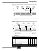
Figure 145. Serial Programming Timing
Note: 2 t
CLCL
for f
ck
< 12 MHz, 3 t
CLCL
for f
ck
>= 12 MHz
Programming Via the
JTAG Interface
Programming through the JTAG interface requires control of the four JTAG specific
pins: TCK, TMS, TDI and TDO. Control of the reset and clock pins is not required.
To be able to use the JTAG interface, the JTAGEN fuse must be programmed. The
device is default shipped with the fuse programmed. In addition, the JTD bit in MCUCSR
must be cleared. Alternatively, if the JTD bit is set, the external reset can be forced low.
Then, the JTD bit will be cleared after two chip clocks, and the JTAG pins are available
for programming. This provides a means of using the JTAG pins as normal port pins in
running mode while still allowing in-system programming via the JTAG interface. Note
that this technique can not be used when using the JTAG pins for Boundary-scan or On-
chip Debug. In these cases the JTAG pins must be dedicated for this purpose.
As a definition in this data sheet, the LSB is shifted in and out first of all shift registers.
Programming Specific JTAG
Instructions
The instruction register is 4-bit wide, supporting up to 16 instructions. The JTAG instruc-
tions useful for Programming are listed below.
The OPCODE for each instruction is shown behind the instruction name in hex format.
The text describes which data register is selected as path between TDI and TDO for
each instruction.
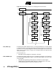
The Run-Test/Idle state of the TAP controller is used to generate internal clocks. It can
also be used as an idle state between JTAG sequences. The state machine sequence
for changing the instruction word is shown in
Figure 146.
Table 131. Serial Programming Characteristics, T
A
= -40°C to 85°C, V
CC
= 2.7V - 5.5V
(Unless Otherwise Noted)
Symbol Parameter Min Typ Max Units
1/t
CLCL
Oscillator Frequency (V
CC
= 2.7 - 5.5 V) 0 TBD MHz
t
CLCL
Oscillator Period (V
CC
= 2.7 - 5.5 V) 250 ns
1/t
CLCL
Oscillator Frequency (V
CC
= 4.5 - 5.5 V) 0 TBD MHz
t
CLCL
Oscillator Period (V
CC
= 4.5 - 5.5 V) 125 ns
t
SHSL
SCK Pulse Width High 2 t
CLCL
* ns
t
SLSH
SCK Pulse Width Low 2 t
CLCL
* ns
t
OVSH
MOSI Setup to SCK High t
CLCL
ns
t
SHOX
MOSI Hold after SCK High 2 t
CLCL
ns
t
SLIV
SCK Low to MISO Valid TBD TBD TBD ns
MOSI
MISO
SCK
t
OVSH
t
SHSL
t
SLSH
t
SHOX
t
SLIV