Features • High-performance, Low-power AVR® 8-bit Microcontroller • Advanced RISC Architecture • • • • • • • – 133 Powerful Instructions – Most Single Clock Cycle Execution – 32 x 8 General Purpose Working Registers + Peripheral Control Registers – Fully Static Operation – Up to 16 MIPS Throughput at 16 MHz – On-chip 2-cycle Multiplier Nonvolatile Program and Data Memories – 128K Bytes of In-System Reprogrammable Flash Endurance: 1,000 Write/Erase Cycles – Optional Boot Code Section with Independent L
Figure 1.
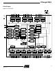
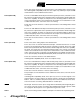
ATmega128(L) Block Diagram PC0 - PC7 PA0 - PA7 RESET XTAL1 PF0 - PF7 XTAL2 Figure 2. Block Diagram VCC GND PORTA DRIVERS PORTF DRIVERS DATA DIR. REG. PORTF DATA REGISTER PORTF PORTC DRIVERS DATA DIR. REG. PORTA DATA REGISTER PORTA DATA REGISTER PORTC DATA DIR. REG. PORTC 8-BIT DATA BUS AVCC CALIB.
The AVR core combines a rich instruction set with 32 general purpose working registers. All the 32 registers are directly connected to the Arithmetic Logic Unit (ALU), allowing two independent registers to be accessed in one single instruction executed in one clock cycle. The resulting architecture is more code efficient while achieving throughputs up to ten times faster than conventional CISC microcontrollers.
ATmega128(L) The ATmega128 is 100% pin compatible with ATmega103, and can replace the ATmega103 on current Printed Circuit Boards. The application note “Replacing ATmega103 by ATmega128” describes what the user should be aware of replacing the ATmega103 by an ATmega128. ATmega103 Compatibility Mode By programming the M103C fuse, the ATmega128 will be compatible with the ATmega103 regards to RAM, I/O pins and interrupt vectors as described above.
Port C also serves the functions of special features of the ATmega128 as listed on page 72. In ATmega103 compatibility mode, Port C is output only, and the port C pins are not tri-stated when a reset condition becomes active. Port D (PD7..PD0) Port D is an 8-bit bidirectional I/O port with internal pull-up resistors (selected for each bit). The Port D output buffers have symmetrical drive characteristics with both high sink and source capability.
ATmega128(L) XTAL2 Output from the inverting oscillator amplifier. AVCC This is the supply voltage pin for Port F and the A/D Converter. It should be externally connected to VCC, even if the ADC is not used. If the ADC is used, it should be connected to VCC through a low-pass filter. AREF This is the analog reference pin for the A/D Converter. PEN This is a programming enable pin for the serial programming mode.
AVR CPU Core Introduction This chapter discusses the AVR core architecture in general. The main function of the CPU core is to ensure correct program execution. The CPU must therefore be able to access memories, perform calculations, control peripherals and handle interrupts. Architectural Overview Figure 3.
ATmega128(L) an arithmetic operation, the Status Register is updated to reflect information about the result of the operation. Program flow is provided by conditional and unconditional jump and call instructions, able to directly address the whole address space. Most AVR instructions have a single 16-bit word format. Every program memory address contains a 16- or 32-bit instruction. Program Flash memory space is divided in two sections, the Boot program section and the Application Program section.
• Bit 7 - I: Global Interrupt Enable The global interrupt enable bit must be set for the interrupts to be enabled. The individual interrupt enable control is then performed in separate control registers. If the global interrupt enable register is cleared, none of the interrupts are enabled independent of the individual interrupt enable settings. The I-bit is cleared by hardware after an interrupt has occurred, and is set by the RETI instruction to enable subsequent interrupts.
ATmega128(L) Figure 4. AVR CPU General Purpose Working Registers 7 0 Addr.
Stack Pointer The stack is mainly used for storing temporary data, for storing local variables and for storing return addresses after interrupts and subroutine calls. The stack pointer register always points to the top of the stack. Note that the stack is implemented as growing from higher memory locations to lower memory locations. This implies that a stack PUSH command decreases the stack pointer. The Stack Pointer points to the data SRAM stack area where the Subroutine and Interrupt Stacks are located.
ATmega128(L) Instruction Execution Timing This section describes the general access timing concepts for instruction execution. The AVR CPU is driven by the CPU clock clkCPU, directly generated from the selected clock source for the chip. No internal clock division is used. Figure 6 shows the parallel instruction fetches and instruction executions enabled by the Harvard architecture and the fast-access Register file concept.
When an interrupt occurs, the Global Interrupt Enable I-bit is cleared and all interrupts are disabled. The user software can write logic one to the I-bit to enable nested interrupts. All enabled interrupts can then interrupt the current interrupt routine. The I-bit is automatically set when a Return from Interrupt instruction – RETI – is executed. There are basically two types of interrupts. The first type is triggered by an event that sets the interrupt flag.
ATmega128(L) Assembly Code Example sei ; set global interrupt enable sleep ; enter sleep, waiting for interrupt ; note: will enter sleep before any pending ; interrupt(s) C Code Example _SEI(); /* set global interrupt enable */ _SLEEP(); /* enter sleep, waiting for interrupt */ /* note: will enter sleep before any pending interrupt(s) */ Interrupt Response Time The interrupt execution response for all the enabled AVR interrupts is 4 clock cycles minimum.
AVR ATmega128 Memories This section describes the different memories in the ATmega128. The AVR architecture has two main memory spaces, the Data Memory and the Program Memory space. In addition, the ATmega128 features an EEPROM Memory for data storage. All three memory spaces are linear and regular. In-System Reprogrammable Flash Program Memory The ATmega128 contains 128K bytes On-chip In-System Reprogrammable Flash memory for program storage.
ATmega128(L) SRAM Data Memory The ATmega128 supports two different configurations for the SRAM data memory as listed in Table 1. Table 1. Memory Configurations Configuration Internal SRAM Data Memory External SRAM Data Memory Normal Mode 4096 up to 64K ATmega103 Compatibility Mode 4000 up to 64K Figure 9 shows how the ATmega128 SRAM Memory is organized.
The five different addressing modes for the data memory cover: Direct, Indirect with Displacement, Indirect, Indirect with Pre-decrement, and Indirect with Post-increment. In the Register file, registers R26 to R31 feature the indirect addressing pointer registers. The direct addressing reaches the entire data space. The Indirect with Displacement mode reaches 63 address locations from the base address given by the Y- or Z-register.
ATmega128(L) Figure 10. On-chip Data SRAM Access Cycles T1 T2 T3 clkCPU Address Address valid Compute Address Write Data WR Read Data RD Memory access instruction EEPROM Data Memory Next instruction The ATmega128 contains 4K bytes of data EEPROM memory. It is organized as a separate data space, in which single bytes can be read and written. The EEPROM has an endurance of at least 100,000 write/erase cycles.
• Bits 11..0 - EEAR11..0: EEPROM Address The EEPROM Address Registers – EEARH and EEARL specify the EEPROM address in the 4K bytes EEPROM space. The EEPROM data bytes are addressed linearly between 0 and 4096. The initial value of EEAR is undefined. A proper value must be written before the EEPROM may be accessed. EEPROM Data Register – EEDR Bit 7 6 5 4 3 2 1 MSB 0 LSB Read/Write R/W R/W R/W R/W R/W R/W R/W R/W Initial value 0 0 0 0 0 0 0 0 EEDR • Bits 7..0 - EEDR7.
ATmega128(L) The EEPROM can not be programmed during a CPU write to the Flash memory. The software must check that the Flash programming is completed before initiating a new EEPROM write. Step 2 is only relevant if the software contains a boot loader allowing the CPU to program the Flash. If the Flash is never being updated by the CPU, step 2 can be omitted. See “Boot Loader Support – Read-While-Write Self-Programming” on page 266 for details about boot programming.
Assembly Code Example EEPROM_write: ; Wait for completion of previous write sbic EECR,EEWE rjmp EEPROM_write ; Set up address (r18:r17) in address register out EEARH, r18 out EEARL, r17 ; Write data (r16) to data register out EEDR,r16 ; Write logical one to EEMWE sbi EECR,EEMWE ; Start eeprom write by setting EEWE sbi EECR,EEWE ret C Code Example void EEPROM_write(unsigned int uiAddress, unsigned char ucData) { /* Wait for completion of previous write */ while(EECR & (1<
ATmega128(L) Assembly Code Example EEPROM_read: ; Wait for completion of previous write sbic EECR,EEWE rjmp EEPROM_read ; Set up address (r18:r17) in address register out EEARH, r18 out EEARL, r17 ; Start eeprom read by writing EERE sbi EECR,EERE ; Read data from data register in r16,EEDR ret C Code Example unsigned char EEPROM_read(unsigned int uiAddress) { /* Wait for completion of previous write */ while(EECR & (1<
I/O Memory The I/O space definition of the ATmega128 is shown in “Register Summary” on page 323. All ATmega128 I/Os and peripherals are placed in the I/O space. All I/O locations may be accessed by the LD/LDS/LDD and ST/STS/STD instructions, transferring data between the 32 general purpose working registers and the I/O space. I/O registers within the address range $00 - $1F are directly bit-accessible using the SBI and CBI instructions.
ATmega128(L) Figure 11. External Memory with Sector Select Memory Configuration A Memory Configuration B 0x0000 0x0000 Internal memory Internal memory 0x0FFF 0x1000 0x10FF 0x1100 Lower sector SRW01 SRW00 SRW10 SRL[2..
The control bits for the External Memory Interface are located in three registers, the MCU Control Register – MCUCR, the External Memory Control Register A – XMCRA, and the External Memory Control Register B – XMCRB. When the XMEM interface is enabled, the XMEM interface will override the setting in the data direction registers that corresponds to the ports dedicated to the XMEM interface. For details about the port override, see the alternate functions in section “I/O-Ports” on page 60.
ATmega128(L) The XMEM interface also provides a bus-keeper on the AD7:0 lines. The bus-keeper can be disabled and enabled in software as described in “External Memory Control Register B – XMCRB” on page 31. When enabled, the bus-keeper will keep the previous value on the AD7:0 bus while these lines are tri-stated by the XMEM interface.
Figure 14. External Data Memory Cycles with SRWn1 = 0 and SRWn0 = 1(1) T1 T2 T3 T4 T5 System Clock (CLKCPU ) ALE A15:8 Prev. addr. DA7:0 Prev. data Address DA7:0 (XMBK = 0) Prev. data Address DA7:0 (XMBK = 1) Prev. data XX Write Address Data WR Address Read Data Data RD Note: 1. SRWn1 = SRW11 (upper sector) or SRW01 (lower sector), SRWn0 = SRW10 (upper sector) or SRW00 (lower sector).
ATmega128(L) Figure 16. External Data Memory Cycles with SRWn1 = 1 and SRWn0 = 1(1) T1 T2 T3 T4 T5 T6 T7 System Clock (CLKCPU ) ALE A15:8 Prev. addr. DA7:0 Prev. data Address DA7:0 (XMBK = 0) Prev. data Address DA7:0 (XMBK = 1) Prev. data XX Write Address Data WR Address Read Data Data RD Note: 1. SRWn1 = SRW11 (upper sector) or SRW01 (lower sector), SRWn0 = SRW10 (upper sector) or SRW00 (lower sector).
• Bit 6..4 - SRL2, SRL1, SRL0: Wait-state Sector Limit It is possible to configure different wait-states for different external memory addresses. The external memory address space can be divided in two sectors that have separate wait-state bits. The SRL2, SRL1, and SRL0 bits select the split of the sectors, see Table 3 and Figure 11. By default, the SRL2, SRL1, and SRL0 bits are set to zero and the entire external memory address space is treated as one sector.
ATmega128(L) • Bit 0 - Res: Reserved Bit This is a reserved bit and will always read as zero. When writing to this address location, write this bit to zero for compatibility with future devices. External Memory Control Register B – XMCRB Bit 7 6 5 4 3 2 1 0 XMBK – – – – XMM2 XMM1 XMM0 Read/Write R/W R R R R R/W R/W R/W Initial value 0 0 0 0 0 0 0 0 XMCRB • Bit 7- XMBK: External Memory Bus-keeper Enable Writing XMBK to one enables the bus keeper on the AD7:0 lines.
Using all 64KB Locations of External Memory Since the external memory is mapped after the internal memory as shown in Figure 11, only 60KB of external memory is available by default (address space 0x0000 to 0x10FF is reserved for internal memory). However, it is possible to take advantage of the entire external memory by masking the higher address bits to zero. This can be done by using the XMMn bits and control by software the most significant bits of the address.
ATmega128(L) System Clock and Clock Options Clock Systems and their Distribution Figure 17 presents the principal clock systems in the AVR and their distribution. All of the clocks need not be active at a given time. In order to reduce power consumption, the clocks to modules not being used can be halted by using different sleep modes, as described in “Power Management and Sleep Modes” on page 41. The clock systems are detailed below. Figure 17.
Asynchronous Timer Clock – clkASY The Asynchronous Timer clock allows the Asynchronous Timer/Counter to be clocked directly from an external 32 kHz clock crystal. The dedicated clock domain allows using this Timer/Counter as a real-time counter even when the device is in sleep mode. ADC Clock – clkADC The ADC is provided with a dedicated clock domain. This allows halting the CPU and I/O clocks in order to reduce noise generated by digital circuitry. This gives more accurate ADC conversion results.
ATmega128(L) For resonators, the maximum frequency is 8 MHz with CKOPT unprogrammed and 16 MHz with CKOPT programmed. C1 and C2 should always be equal for both crystals and resonators. The optimal value of the capacitors depends on the crystal or resonator in use, the amount of stray capacitance, and the electromagnetic noise of the environment. Some initial guidelines for choosing capacitors for use with crystals are given in Table 8.
Table 9. Start-up Times for the Crystal Oscillator Clock Selection CKSEL0 0 0 0 0 1 1 1 1 Notes: Low-frequency Crystal Oscillator Start-up Time from Power-down and Power-save SUT1..0 Additional Delay from Reset (VCC = 5.
ATmega128(L) Note: External RC Oscillator 1. These options should only be used if frequency stability at start-up is not important for the application. For timing insensitive applications, the external RC configuration shown in Figure 19 can be used. The frequency is roughly estimated by the equation f = 1/(3RC). C should be at least 22 pF. By programming the CKOPT fuse, the user can enable an internal 36 pF capacitor between XTAL1 and GND, thereby removing the need for an external capacitor.
Calibrated Internal RC Oscillator The calibrated internal RC oscillator provides a fixed 1.0 MHz, 2.0 MHz, 4.0 MHz, or 8.0 MHz clock. All frequencies are nominal values at 5V and 25 °C. This clock may be selected as the system clock by programming the CKSEL fuses as shown in Table 13. If selected, it will operate with no external components. The CKOPT fuse should always be unprogrammed when using this clock option.
ATmega128(L) Table 15. Internal RC Oscillator Frequency Range. External Clock OSCCAL Value Min Frequency in Percentage of Nominal Frequency (%) Max Frequency in Percentage of Nominal Frequency (%) $00 50 100 $7F 75 150 $FF 100 200 To drive the device from an external clock source, XTAL1 should be driven as shown in Figure 20 . To run the device on an external clock, the CKSEL fuses must be programmed to “0000”.
• Bit 7 - XDIVEN: XTAL Divide Enable When the XDIVEN bit is written one, the clock frequency of the CPU and all peripherals (clkI/O, clkADC, clkCPU, clkFLASH) is divided by the factor defined by the setting of XDIV6 XDIV0. This bit can be written run-time to vary the clock frequency as suitable to the application. • Bits 6..0 - XDIV6..XDIV0: XTAL Divide Select Bits 6 - 0 These bits define the division factor that applies when the XDIVEN bit is set (one).
ATmega128(L) Power Management and Sleep Modes Sleep modes enable the application to shut down unused modules in the MCU, thereby saving power. The AVR provides various sleep modes allowing the user to tailor the power consumption to the application’s requirements. To enter any of the six sleep modes, the SE bit in MCUCR must be written to logic one and a SLEEP instruction must be executed.
Idle Mode When the SM2..0 bits are written to 000, the SLEEP instruction makes the MCU enter Idle Mode, stopping the CPU but allowing SPI, USART, Analog Comparator, ADC, 2wire Serial Interface, Timer/Counters, Watchdog, and the interrupt system to continue operating. This sleep mode basically halts clkCPU and clkFLASH, while allowing the other clocks to run.
ATmega128(L) asynchronous timer should be considered undefined after wake-up in Power-save Mode if AS0 is 0. This sleep mode basically halts all clocks except clkASY, allowing operation only of asynchronous modules, including Timer/Counter0 if clocked asynchronously. Standby Mode When the SM2..0 bits are 110 and an external crystal/resonator clock option is selected, the SLEEP instruction makes the MCU enter Standby Mode.
Minimizing Power Consumption There are several issues to consider when trying to minimize the power consumption in an AVR controlled system. In general, sleep modes should be used as much as possible, and the sleep mode should be selected so that as few as possible of the device’s functions are operating. All functions not needed should be disabled. In particular, the following modules may need special consideration when trying to achieve the lowest possible power consumption.
ATmega128(L) System Control and Reset Resetting the AVR During reset, all I/O registers are set to their initial values, and the program starts execution from the Reset Vector. The instruction placed at the Reset Vector must be a JMP absolute jump - instruction to the reset handling routine. If the program never enables an interrupt source, the interrupt vectors are not used, and regular program code can be placed at these locations.
Figure 21. Reset Logic DATA BUS D Q L Q MCU Control and Status Register (MCUCSR) PORF BORF EXTRF WDRF JTRF PEN Pull-up Resistor Power-On Reset Circuit Brown-Out Reset Circuit BODEN BODLEVEL Pull-up Resistor SPIKE FILTER JTAG Reset Register Reset Circuit COUNTER RESET RESET Watchdog Timer Watchdog Oscillator Clock Generator CK Delay Counters TIMEOUT CKSEL[3:0] SUT[1:0] Table 19. Reset Characteristics(1) Symbol Min Typ Max Units Power-on Reset Threshold Voltage (rising) TBD TBD 2.
ATmega128(L) Power-on Reset A Power-on Reset (POR) pulse is generated by an on-chip detection circuit. The detection level is defined in Table 19 . The POR is activated whenever VCC is below the detection level. The POR circuit can be used to trigger the start-up reset, as well as to detect a failure in supply voltage. A Power-on Reset (POR) circuit ensures that the device is reset from power-on.
Figure 24. External Reset During Operation CC Brown-out Detection ATmega128 has an on-chip brown-out detection (BOD) circuit for monitoring the VCC level during operation by comparing it to a fixed trigger level. The trigger level for the BOD can be selected by the fuse BODLEVEL to be 2.7V (BODLEVEL unprogrammed), or 4.0V (BODLEVEL programmed). The trigger level has a hysteresis to ensure spike free brown-out detection.
ATmega128(L) Figure 26. Watchdog Reset During Operation CC CK MCU Control and Status Register – MCUCSR The MCU Control and Status Register provides information on which reset source caused an MCU reset. Bit 7 6 5 4 3 2 1 0 JTD - - JTRF WDRF BORF EXTRF PORF Read/Write R/W R R R/W R/W R/W R/W R/W Initial value 0 0 0 MCUCSR See bit description Note that only EXTRF and PORF are available in ATmega103 compatibility mode.
Voltage Reference Enable Signals and Start-up Time The voltage reference has a start-up time that may influence the way it should be used. The start-up time is given in Table 20. To save power, the reference is not always turned on. The reference is on during the following situations: 1. When the BOD is enabled (by programming the BODEN fuse). 2. When the bandgap reference is connected to the Analog Comparator (by setting the ACBG bit in ACSR). 3. When the ADC is enabled.
ATmega128(L) Table 21. WDT Configuration as a Function of the Fuse Settings of M103C and WDTON. Safety Level WDT Initial State How to Disable the WDT How to Change Time-out M103C WDTON Unprogrammed Unprogrammed 1 Disabled Timed sequence Timed sequence Unprogrammed Programmed 2 Enabled Always enabled Timed sequence Programmed Unprogrammed 0 Disabled Timed sequence No restriction Programmed Programmed 2 Enabled Always enabled Timed sequence Figure 27.
1. In the same operation, write a logic one to WDCE and WDE. A logic one must be written to WDE even though it is set to one before the disable operation starts. 2. Within the next four clock cycles, write a logic 0 to WDE. This disables the watchdog. In safety level 2, it is not possible to disable the Watchdog Timer, even with the algorithm described above. See “Timed Sequences for Changing the Configuration of the Watch Dog Timer” on page 53. • Bits 2..
ATmega128(L) Timed Sequences for Changing the Configuration of the Watch Dog Timer The sequence for changing configuration differs slightly between the 3 safety levels. Separate procedures are described for each level. Safety Level 0 This mode is compatible with the watchdog operation found in ATmega103. The watchdog timer is initially disabled, but can be enabled by writing the WDE bit to 1 without any restriction. The time-out period can be changed at any time without restriction.
Interrupts Interrupt Vectors in ATmega128 This chapter describes the specifics of the interrupt handling as performed in ATmega128. For a general explanation of the AVR interrupt handling, refer to “Reset and Interrupt Handling” on page 13. Table 23. Reset and Interrupt Vectors Vector No.
ATmega128(L) Table 23. Reset and Interrupt Vectors (Continued) Vector No. Program Address(2) 31 Source Interrupt Definition $003C(3) USART1, RX USART1, Rx Complete 32 $003E(3) USART1, UDRE USART1 Data Register Empty 33 (3) USART1, TX USART1, Tx Complete (3) $0040 34 $0042 TWI 2-wire Serial Interface 35 $0044(3) SPM READY Store Program Memory Ready Notes: 1.
The most typical and general program setup for the Reset and Interrupt Vector Addresses in ATmega128 is: Address Labels Code Comments $0000 jmp RESET ; Reset Handler $0002 jmp EXT_INT0 ; IRQ0 Handler $0004 jmp EXT_INT1 ; IRQ1 Handler $0006 jmp EXT_INT2 ; IRQ2 Handler $0008 jmp EXT_INT3 ; IRQ3 Handler $000A jmp EXT_INT4 ; IRQ4 Handler $000C jmp EXT_INT5 ; IRQ5 Handler $000E jmp EXT_INT6 ; IRQ6 Handler $0010 jmp EXT_INT7 ; IRQ7 Handler $0012 jmp TIM2_COMP ; Timer2 Comp
ATmega128(L) When the BOOTRST fuse is unprogrammed, the boot section size set to 8K bytes and the IVSEL bit in the MCUCR register is set before any interrupts are enabled, the most typical and general program setup for the Reset and Interrupt Vector Addresses is: Address Labels Code $0000 RESET:ldi Comments $0001 out SPH,r16 $0002 ldi r16,low(RAMEND) $0003 $0004 out sei SPL,r16 $0005 xxx r16,high(RAMEND) ; Main program start ; Set stack pointer to top of RAM ; Enable interrupts ;
Moving Interrupts Between Application and Boot Space MCU Control Register – MCUCR The General Interrupt Control Register controls the placement of the interrupt vector table. Bit 7 6 5 4 3 2 1 0 SRE SRW10 SE SM1 SM0 SM2 IVSEL IVCE Read/Write R/W R/W R/W R/W R/W R/W R/W R/W Initial value 0 0 0 0 0 0 0 0 MCUCR • Bit 1 - IVSEL: Interrupt Vector Select When the IVSEL bit is cleared (zero), the interrupt vectors are placed at the start of the Flash memory.
ATmega128(L) • Bit 0 - IVCE: Interrupt Vector Change Enable The IVCE bit must be written to logic one to enable change of the IVSEL bit. IVCE is cleared by hardware four cycles after it is written or when IVSEL is written. Setting the IVCE bit will disable interrupts, as explained in the IVSEL description above. See Code Example below.
I/O-Ports Introduction All AVR ports have true Read-Modify-Write functionality when used as general digital I/O ports. This means that the direction of one port pin can be changed without unintentionally changing the direction of any other pin with the SBI and CBI instructions. The same applies when changing drive value (if configured as output) or enabling/disabling of pull-up resistors (if configured as input).
ATmega128(L) Ports as General Digital I/O The ports are bi-directional I/O ports with optional internal pull-ups. Figure 29 shows a functional description of one I/O port pin, here generically called Pxn. Figure 29.
When switching between tri-state ({DDxn, PORTxn} = 0b00) and output high ({DDxn, PORTxn} = 0b11), an intermediate state with either pull-up enabled ({DDxn, PORTxn} = 0b01) or output low ({DDxn, PORTxn} = 0b10) must occur. Normally, the pull-up enabled state is fully acceptable, as a high-impedant environment will not notice the difference between a strong high driver and a pull-up. If this is not the case, the PUD bit in the SFIOR register can be written to one to disable all pull-ups in all ports.
ATmega128(L) Figure 30. Synchronization when Reading an Externally Applied Pin Value SYSTEM CLK INSTRUCTIONS XXX XXX in r17, PINx SYNC LATCH PINxn r17 0x00 0xFF tpd, max tpd, min Consider the clock period starting shortly after the first falling edge of the system clock. The latch is closed when the clock is low, and goes transparent when the clock is high, as indicated by the shaded region of the “SYNC LATCH” signal. The signal value is latched when the system clock goes low.
Figure 31. Synchronization when Reading a Software Assigned Pin Value SYSTEM CLK r16 INSTRUCTIONS 0xFF out PORTx, r16 nop in r17, PINx SYNC LATCH PINxn r17 0x00 0xFF tpd The following code example shows how to set port B pins 0 and 1 high, 2 and 3 low, and define the port pins from 4 to 7 as input with pull-ups assigned to port pins 6 and 7.
ATmega128(L) Assembly Code Example(1) ... ; Define pull-ups and set outputs high ; Define directions for port pins ldi r16,(1<
Alternate Port Functions Most port pins have alternate functions in addition to being general digital I/Os. Figure 32 shows how the port pin control signals from the simplified Figure 29 can be overridden by alternate functions. The overriding signals may not be present in all port pins, but the figure serves as a generic description applicable to all port pins in the AVR microcontroller family. Figure 32.
ATmega128(L) Table 26. Generic Description of Overriding Signals for Alternate Functions. Signal Name Full Name Description PUOE Pull-up Override Enable If this signal is set, the pull-up enable is controlled by the PUOV signal. If this signal is cleared, the pull-up is enabled when {DDxn, PORTxn, PUD} = 0b010. PUOV Pull-up Override Value If PUOE is set, the pull-up is enabled/disabled when PUOV is set/cleared, regardless of the setting of the DDxn, PORTxn, and PUD register bits.
• Bit 2 - PUD: Pull-up disable When this bit is written to one, the pull-ups in the I/O ports are disabled even if the DDxn and PORTxn registers are configured to enable the pull-ups ({DDxn, PORTxn} = 0b01). See “Configuring the Pin” on page 61 for more details about this feature. Alternate Functions of Port A The Port A has an alternate function as the address low byte and data lines for the External Memory Interface. Table 27.
ATmega128(L) Table 29. Overriding Signals for Alternate Functions in PA3..
• OC1B, Bit 6 OC1B, Output Compare matchB output: The PB6 pin can serve as an external output for the Timer/Counter1 output compareB. The pin has to be configured as an output (DDB6 set (one)) to serve this function. The OC1B pin is also the output pin for the PWM mode timer function. • OC1A, Bit 5 OC1A, Output Compare matchA output: The PB5 pin can serve as an external output for the Timer/Counter1 output compareA. The pin has to be configured as an output (DDB5 set (one)) to serve this function.
ATmega128(L) Table 31. Overriding Signals for Alternate Functions in PB7..PB4 Signal Name PB7/OC2/OC1C PB6/OC1B PB5/OC1A PB4/OC0 PUOE 0 0 0 0 PUOV 0 0 0 0 DDOE 0 0 0 0 DDOV 0 0 0 0 (1) PVOE OC2/OC1C ENABLE OC1B ENABLE OC1A ENABLE OC0 ENABLE PVOV OC2/OC1C(1) OC1B OC1A OC0B DIEOE 0 0 0 0 DIEOV 0 0 0 0 DI – – – – AIO – – – – Note: 1. See “Output Compare Modulator (OCM1C2)” on page 155 for details. OC1C does not exist in ATmega103 compatibility mode.
Alternate Functions of Port C In ATmega103 compatibility mode, Port C is output only. The Port C has an alternate function as the address high byte for the External Memory Interface. Table 33. Port C Pins Alternate Functions Port Pin Alternate Function PC7 A15 PC6 A14 PC5 A13 PC4 A12 PC3 A11 PC2 A10 PC1 A9 PC0 A8 Table 34 and Table 35 relate the alternate functions of Port C to the overriding signals shown in Figure 32 on page 66. Table 34.
ATmega128(L) Table 35. Overriding Signals for Alternate Functions in PC3..PC0(1) Signal Name PC3/A11 PC2/A10 PC1/A9 PC0/A8 PUOE SRE • (XMM<5) SRE • (XMM<6) SRE • (XMM<7) SRE • (XMM<7) PUOV 0 0 0 0 DDOE SRE • (XMM<5) SRE • (XMM<6) SRE • (XMM<7) SRE • (XMM<7) DDOV 1 1 1 1 PVOE SRE • (XMM<5) SRE • (XMM<6) SRE • (XMM<7) SRE • (XMM<7) PVOV A11 A10 A9 A8 DIEOE 0 0 0 0 DIEOV 0 0 0 0 DI – – – – AIO – – – – Note: Alternate Functions of Port D 1.
• IC1 - Port D, Bit 4 IC1 - Input Capture Pin1: The PD4 pin can act as an input capture pin for Timer/Counter1. • INT3/TXD1 - Port D, Bit 3 INT3, External Interrupt source 3: The PD3 pin can serve as an external interrupt source to the MCU. TXD1, Transmit Data (Data output pin for the USART1). When the USART1 transmitter is enabled, this pin is configured as an output regardless of the value of DDD3. • INT2/RXD1 - Port D, Bit 2 INT2, External Interrupt source 2.
ATmega128(L) Table 37. Overriding Signals for Alternate Functions PD7..PD4 Signal Name PD7/T2 PD6/T1 PD5/XCK1 PD4/IC1 PUOE 0 0 0 0 PUOV 0 0 0 0 DDOE 0 0 0 0 DDOV 0 0 0 0 PVOE 0 0 UMSEL1 0 PVOV 0 0 XCK1 OUTPUT 0 DIEOE 0 0 0 0 DIEOV 0 0 0 0 DI T2 INPUT T1 INPUT XCK1 INPUT IC1 INPUT AIO – – – – Table 38. Overriding Signals for Alternate Functions in PD3..
Alternate Functions of Port E The Port E pins with alternate functions are shown in Table 39. Table 39.
ATmega128(L) OC3A, Output Compare matchA output: The PE3 pin can serve as an external output for the Timer/Counter3 output compareA. The pin has to be configured as an output (DDE3 set “one”) to serve this function. The OC3A pin is also the output pin for the PWM mode timer function. • AIN0/XCK0 - Port E, Bit 2 AIN0 - Analog Comparator Positive Input. This pin is directly connected to the positive input of the analog comparator. XCK0, USART0 external clock.
Table 41. Overriding Signals for Alternate Functions in PE3..
ATmega128(L) • TMS, ADC5 - Port F, Bit 5 ADC5, Analog to Digital Converter, Channel 5. TMS, JTAG Test Mode Select: This pin is used for navigating through the TAP-controller state machine. When the JTAG interface is enabled, this pin can not be used as an I/O pin. • TDO, ADC4 - Port F, Bit 4 ADC4, Analog to Digital Converter, Channel 4. TCK, JTAG Test Clock: JTAG operation is synchronous to TCK. When the JTAG interface is enabled, this pin can not be used as an I/O pin. • ADC3 - ADC0 - Port F, Bit 3..
Alternate Functions of Port G In ATmega103 compatibility mode, only the alternate functions are the defaults for Port G, and Port G cannot be used as General Digital Port Pins. The alternate pin configuration is as follows: Table 45.
ATmega128(L) Table 47.
Port B Input Pins Address – PINB Bit 7 6 5 4 3 2 1 0 PINB7 PINB6 PINB5 PINB4 PINB3 PINB2 PINB1 PINB0 Read/Write R R R R R R R R Initial value N/A N/A N/A N/A N/A N/A N/A N/A PINB Port C Data Register – PORTC Bit Port C Data Direction Register – DDRC Port C Input Pins Address – PINC 7 6 5 4 3 2 1 0 PORTC7 PORTC6 PORTC5 PORTC4 PORTC3 PORTC2 PORTC1 PORTC0 Read/Write R/W R/W R/W R/W R/W R/W R/W R/W Initial value 0 0 0 0 0 0 0 0 Bit 7 6
ATmega128(L) Port E Data Direction Register – DDRE Port E Input Pins Address – PINE Bit 7 6 5 4 3 2 1 0 DDE7 DDE6 DDE5 DDE4 DDE3 DDE2 DDE1 DDE0 Read/Write R/W R/W R/W R/W R/W R/W R/W R/W Initial value 0 0 0 0 0 0 0 0 Bit 7 6 5 4 3 2 1 0 PINE7 PINE6 PINE5 PINE4 PINE3 PINE2 PINE1 PINE0 Read/Write R R R R R R R R Initial value N/A N/A N/A N/A N/A N/A N/A N/A DDRE PINF Port F Data Register – PORTF Bit Port F Data Direction Register – DDR
External Interrupts The external interrupts are triggered by the INT7:0 pins. Observe that, if enabled, the interrupts will trigger even if the INT7:0 pins are configured as outputs. This feature provides a way of generating a software interrupt. The external interrupts can be triggered by a falling or rising edge or a low level. This is set up as indicated in the specification for the External Interrupt Control Registers – EICRA (INT3:0) and EICRB (INT7:4).
ATmega128(L) Table 48. Interrupt Sense Control(1) ISCn1 ISCn0 0 0 The low level of INTn generates an interrupt request. 0 1 Reserved 1 0 The falling edge of INTn generates asynchronously an interrupt request. 1 Note: Description 1 The rising edge of INTn generates asynchronously an interrupt request. 1. n = 3, 2, 1or 0. When changing the ISCn1/ISCn0 bits, the interrupt must be disabled by clearing its Interrupt Enable bit in the EIMSK Register.
External Interrupt Mask Register – EIMSK Bit 7 6 5 4 3 2 1 0 INT7 INT6 INT5 INT4 INT3 INT2 INT1 IINT0 Read/Write R/W R/W R/W R/W R/W R/W R/W R/W Initial value 0 0 0 0 0 0 0 0 EIMSK • Bits 7..4 - INT7 - INT0: External Interrupt Request 7 - 0 Enable When an INT7- INT4 bit is written to one and the I-bit in the Status Register (SREG) is set (one), the corresponding external pin interrupt is enabled.
ATmega128(L) 8-bit Timer/Counter0 with PWM and Asynchronous Operation Timer/Counter0 is a general purpose, single channel, 8-bit Timer/Counter module.
The Timer/Counter can be clocked internally, via the prescaler, or asynchronously clocked from the TOSC1/2 pins, as detailed later in this chapter. The asynchronous operation is controlled by the Asynchronous Status Register (ASSR). The Clock Select logic block controls which clock source the Timer/Counter uses to increment (or decrement) its value. The Timer/Counter is inactive when no clock source is selected. The output from the clock select logic is referred to as the timer clock (clkT0).
ATmega128(L) Signal description (internal signals): count Increment or decrement TCNT0 by 1. direction Selects between increment and decrement. clear Clear TCNT0 (set all bits to zero). clkT0 Timer/counter clock. top Signalizes that TCNT0 has reached maximum value. bottom Signalizes that TCNT0 has reached minimum value (zero). Depending on the mode of operation used, the counter is cleared, incremented, or decremented at each timer clock (clkT0).
Figure 35. Output Compare Unit, Block Diagram DATA BUS OCRn TCNTn = (8-bit Comparator ) OCFn (Int.Req.) top bottom Waveform Generator OCxy FOCn WGMn1:0 COMn1:0 The OCR0 register is double buffered when using any of the pulse width modulation (PWM) modes. For the normal and clear timer on compare (CTC) modes of operation, the double buffering is disabled. The double buffering synchronizes the update of the OCR0 compare register to either top or bottom of the counting sequence.
ATmega128(L) The setup of the OC0 should be performed before setting the data direction register for the port pin to output. The easiest way of setting the OC0 value is to use the force output compare (FOC0) strobe bit in normal mode. The OC0 register keeps its value even when changing between waveform generation modes. Be aware that the COM01:0 bits are not double buffered together with the compare value. Changing the COM01:0 bits will take effect immediately.
mode, refer to Table 54 on page 99, and for phase correct PWM refer to Table 55 on page 100. A change of the COM01:0 bits state will have effect at the first compare match after the bits are written. For non-PWM modes, the action can be forced to have immediate effect by using the FOC0 strobe bits. Modes of Operation The mode of operation, i.e.
ATmega128(L) Figure 37. CTC Mode, Timing Diagram OCn Interrupt Flag Set TCNTn OCn (Toggle) Period (COMn1:0 = 1) 1 2 3 4 An interrupt can be generated each time the counter value reaches the TOP value by using the OCF0 flag. If the interrupt is enabled, the interrupt handler routine can be used for updating the TOP value.
non-inverted and inverted PWM outputs. The small horizontal line marks on the TCNT0 slopes represent compare matches between OCR0 and TCNT0. Figure 38. Fast PWM Mode, Timing Diagram OCRn Interrupt Flag Set OCRn Update and TOVn Interrupt Flag Set TCNTn OCn (COMn1:0 = 2) OCn (COMn1:0 = 3) Period 1 2 3 4 5 6 7 The Timer/Counter overflow flag (TOV0) is set each time the counter reaches Max If the interrupt is enabled, the interrupt handler routine can be used for updating the compare value.
ATmega128(L) Phase Correct PWM Mode The phase correct PWM mode (WGM01:0 = 3) provides a high resolution phase correct PWM waveform generation option. The phase correct PWM mode is based on a dualslope operation. The counter counts repeatedly from BOTTOM to MAX and then from MAX to BOTTOM. In non-inverting compare output mode, the output compare (OC0) is cleared on the compare match between TCNT0 and OCR0 while upcounting, and set on the compare match while downcounting.
and TCNT0 when the counter decrements. The PWM frequency for the output when using phase correct PWM can be calculated by the following equation: f clk_I/O f OCnPCPWM = ----------------N ⋅ 510 The N variable represents the prescale factor (1, 8, 32, 64, 128, 256, or 1024). The extreme values for the OCR0 register represent special cases when generating a PWM waveform output in the phase correct PWM mode.
ATmega128(L) Figure 41. Timer/Counter Timing Diagram, with Prescaler (fclk_I/O/8) clkI/O clkTn (clkI/O /8) TCNTn MAX - 1 MAX BOTTOM BOTTOM + 1 TOVn Figure 42 shows the setting of OCF0 in all modes except CTC mode. Figure 42. Timer/Counter Timing Diagram, Setting of OCF0, With Prescaler (fclk_I/O/8) clkI/O clkTn (clkI/O /8) TCNTn OCRn OCRn - 1 OCRn OCRn + 1 OCRn + 2 OCRn Value OCFn Figure 43 shows the setting of OCF0 and the clearing of TCNT0 in CTC mode.
Figure 43.
ATmega128(L) Table 52. Waveform Generation Mode Bit Description Mode WGM01(1) (CTC0) WGM00(1) (PWM0) 0 0 1 Timer/Counter Mode of Operation TOP Update of OCR0 at TOV0 Flag Set on 0 Normal 0xFF Immediate MAX 0 1 PWM, Phase Correct 0xFF TOP BOTTOM 2 1 0 CTC OCR0 Immediate MAX 3 1 1 Fast PWM 0xFF TOP MAX Note: 1. The CTC0 and PWM0 bit definition names are now obsolete. Use the WGM01:0 definitions.
Table 55. Compare Output Mode, Phase Correct PWM Mode(1) COM01 COM00 0 0 Normal port operation, OC0 disconnected. 0 1 Reserved 1 0 Clear OC0 on compare match when up-counting. Set OC0 on compare match when downcounting. 1 1 Set OC0 on compare match when up-counting. Clear OC0 on compare match when downcounting. Note: Description 1. A special case occurs when OCR0 equals TOP and COM01 is set. In this case, the compare match is ignored, but the set or clear is done at TOP.
ATmega128(L) Asynchronous Operation of the Timer/Counter Asynchronous Status Register – ASSR Bit 7 6 5 4 3 2 1 0 - - - - AS0 TCN0UB OCR0UB TCR0UB Read/Write R R R R R/W R R R Initial value 0 0 0 0 0 0 0 0 ASSR • Bit 3 - AS0: Asynchronous Timer/Counter0 When AS0 is written to zero, Timer/Counter0 is clocked from the I/O clock, clkI/O. When AS0 is written to one, Timer/Counter 0 is clocked from a crystal oscillator connected to the Timer Oscillator 1 (TOSC1) pin.
• The oscillator is optimized for use with a 32.768 kHz watch crystal. Applying an external clock to the TOSC1 pin may result in incorrect Timer/Counter0 operation. The CPU main clock frequency must be more than four times the oscillator frequency. • When writing to one of the registers TCNT0, OCR0, or TCCR0, the value is transferred to a temporary register, and latched after two positive edges on TOSC1.
ATmega128(L) read as the previous value (before entering sleep) until the next rising TOSC1 edge. The phase of the TOSC clock after waking up from Power-save mode is essentially unpredictable, as it depends on the wake-up time. The recommended procedure for reading TCNT0 is thus as follows: 1. Write any value to either of the registers OCR0 or TCCR0. 2. Wait for the corresponding Update Busy Flag to be cleared. 3. Read TCNT0.
Figure 44. Prescaler for Timer/Counter0 clkT0S PSR0 clkT0S/1024 clkT0S/128 clkT0S/8 AS0 clkT0S/256 10-BIT T/C PRESCALER Clear TOSC1 clkT0S/64 clkOSC clkT0S/32 Timer/Counter Prescaler 0 CS00 CS01 CS02 TIMER/COUNTER0 CLOCK SOURCE clkT0 The clock source for Timer/Counter0 is named clkT0S. clkT0S is by default connected to the main system clock clkOSC. By setting the AS0 bit in ASSR, Timer/Counter0 is asynchronously clocked from the TOSC1 pin.
ATmega128(L) • Bit 1 - PSR0: Prescaler Reset Timer/Counter0 When this bit is written to one, the Timer/Counter0 prescaler will be reset. The bit will be cleared by hardware after the operation is performed. Writing a zero to this bit will have no effect. This bit will always be read as zero if Timer/Counter0 is clocked by the internal CPU clock. If this bit is written when Timer/Counter0 is operating in asynchronous mode, the bit will remain one until the prescaler has been reset.
16-bit Timer/Counter (Timer/Counter1 and Timer/Counter3) The 16-bit Timer/Counter unit allows accurate program execution timing (event management), wave generation, and signal timing measurement. The main features are: • True 16-bit Design (i.e.
ATmega128(L) Figure 45. 16-bit Timer/Counter Block Diagram Count Clear Direction TOVx (Int.Req.) Control Logic TCLK Clock Select Edge Detector TOP BOTTOM ( From Prescaler ) Timer/Counter TCNTx Tx = =0 OCFxA (Int.Req.) Waveform Generation = OCxA OCRxA OCFxB (Int.Req.) Fixed TOP Values Waveform Generation DATABUS = OCxB OCRxB OCFxC (Int.Req.) Waveform Generation = OCRxC ( From Analog Comparator Ouput ) ICFx (Int.Req.
The double buffered Output Compare Registers (OCRnA/B/C) are compared with the Timer/Counter value at all time. The result of the compare can be used by the waveform generator to generate a PWM or variable frequency output on the Output Compare Pin (OCnA/B/C). See “Output Compare Units” on page 115.. The compare match event will also set the compare match flag (OCFnA/B/C) which can be used to generate an output compare interrupt request.
ATmega128(L) • WGMn3 is added to TCCRnB. Interrupt flag and mask bits for output compare unit C are added. The 16-bit Timer/Counter has improvements that will affect the compatibility in some special cases. Accessing 16-bit Registers The TCNTn, OCRnA/B/C, and ICRn are 16-bit registers that can be accessed by the AVR CPU via the 8-bit data bus. The 16-bit register must be byte accessed using two read or write operations.
It is important to notice that accessing 16-bit registers are atomic operations. If an interrupt occurs between the two instructions accessing the 16-bit register, and the interrupt code updates the temporary register by accessing the same or any other of the 16-bit timer registers, then the result of the access outside the interrupt will be corrupted. Therefore, when both the main code and the interrupt code update the temporary register, the main code must disable the interrupts during the 16-bit access.
ATmega128(L) The following code examples show how to do an atomic write of the TCNTn register contents. Writing any of the OCRnA/B/C or ICRn registers can be done by using the same principle.
Figure 46. Counter Unit Block Diagram DATABUS (8-bit) TOVn (Int.Req.) TEMP (8-bit) Clock Select Count TCNTnH (8-bit) TCNTnL (8-bit) TCNTn (16-bit Counter) Clear Direction Control Logic clkTn Edge Detector Tn ( From Prescaler ) TOP BOTTOM Signal description (internal signals): Count Increment or decrement TCNTn by 1. Direction Select between increment and decrement. Clear Clear TCNTn (set all bits to zero). clkTn Timer/counter clock. TOP Signalize that TCNTn has reached maximum value.
ATmega128(L) Input Capture Unit The Timer/Counter incorporates an input capture unit that can capture external events and give them a time-stamp indicating time of occurrence. The external signal indicating an event, or multiple events, can be applied via the ICPn pin or alternatively, for the Timer/Counter1 only, via the analog-comparator unit. The time-stamps can then be used to calculate frequency, duty-cycle, and other features of the signal applied.
written to the ICRn register. When writing the ICRn register the high byte must be written to the ICRnH I/O location before the low byte is written to ICRnL. For more information on how to access the 16-bit registers refer to “Accessing 16-bit Registers” on page 109. Input Capture Trigger Source The main trigger source for the input capture unit is the input capture pin (ICPn). Timer/counter 1 can alternatively use the analog comparator output as trigger source for the input capture unit.
ATmega128(L) Output Compare Units The 16-bit comparator continuously compares TCNTn with the output compare register (OCRnx). If TCNT equals OCRnx the comparator signals a match. A match will set the output compare flag (OCFnx) at the next timer clock cycle. If enabled (OCIEnx = 1), the output compare flag generates an output compare interrupt. The OCFnx flag is automatically cleared when the interrupt is executed.
sequence. The synchronization prevents the occurrence of odd-length, non-symmetrical PWM pulses, thereby making the output glitch-free. The OCRnx register access may seem complex, but this is not case. When the double buffering is enabled, the CPU has access to the OCRnx buffer register, and if double buffering is disabled the CPU will access the OCRnx directly.
ATmega128(L) internal OCnx register, not the OCnx pin. If a system reset occur, the OCnx register is reset to “0”. Figure 49. Compare Match Output Unit, Schematic COMnx1 COMnx0 FOCnx Waveform Generator D Q 1 OCnx DATABUS D 0 OCnx Pin Q PORT D Q DDR clk I/O The general I/O port function is overridden by the output compare (OCnx) from the waveform generator if either of the COMnx1:0 bits are set.
inverted PWM). For non-PWM modes the COMnx1:0 bits control whether the output should be set, cleared or toggle at a compare match (See “Compare Match Output Unit” on page 116.) For detailed timing information refer to “Timer/Counter Timing Diagrams” on page 125. Normal Mode The simplest mode of operation is the normal mode (WGMn3:0 = 0). In this mode the counting direction is always up (incrementing), and no counter clear is performed.
ATmega128(L) counter is running with none or a low prescaler value must be done with care since the CTC mode does not have the double buffering feature. If the new value written to OCRnA or ICRn is lower than the current value of TCNTn, the counter will miss the compare match. The counter will then have to count to its maximum value (0xFFFF) and wrap around starting at 0x0000 before the compare match can occur. In many cases this feature is not desirable.
Figure 51. Fast PWM Mode, Timing Diagram OCRnx / TOP Update and TOVn Interrupt Flag Set and OCnA Interrupt Flag Set or ICFn Interrupt Flag Set (Interrupt on TOP) TCNTn OCnx (COMnx1:0 = 2) OCnx (COMnx1:0 = 3) Period 1 2 3 4 5 6 7 8 The Timer/Counter overflow flag (TOVn) is set each time the counter reaches TOP. In addition the OCnA or ICFn flag is set at the same timer clock cycle as TOVn is set when either OCRnA or ICRn is used for defining the TOP value.
ATmega128(L) setting (or clearing) the OCnx register at the compare match between OCRnx and TCNTn, and clearing (or setting) the OCnx register at the timer clock cycle the counter is cleared (changes from TOP to BOTTOM). The PWM frequency for the output can be calculated by the following equation: f clk_I/O f OCnxPWM = ---------------------------------N ⋅ ( 1 + TOP ) The N variable represents the prescaler divider (1, 8, 64, 256, or 1024).
Figure 52. Phase Correct PWM Mode, Timing Diagram OCRnx / TOP Update and OCnA Interrupt Flag Set or ICFn Interrupt Flag Set (Interrupt on TOP) TOVn Interrupt Flag Set (Interrupt on Bottom) TCNTn OCnx (COMnx1:0 = 2) OCnx (COMnx1:0 = 3) Period 1 2 3 4 The Timer/Counter overflow flag (TOVn) is set each time the counter reaches BOTTOM.
ATmega128(L) match between OCRnx and TCNTn when the counter decrements. The PWM frequency for the output when using phase correct PWM can be calculated by the following equation: f clk_I/O f OCnxPCPWM = --------------------------2 ⋅ N ⋅ TOP The N variable represents the prescaler divider (1, 8, 64, 256, or 1024). The extreme values for the OCRnx register represents special cases when generating a PWM waveform output in the phase correct PWM mode.
Figure 53. Phase and Frequency Correct PWM Mode, Timing Diagram OCnA Interrupt Flag Set or ICFn Interrupt Flag Set (Interrupt on TOP) OCRnx / TOP Update and TOVn Interrupt Flag Set (Interrupt on Bottom) TCNTn OCnx (COMnx1:0 = 2) OCnx (COMnx1:0 = 3) Period 1 2 3 4 The Timer/Counter overflow flag (TOVn) is set at the same timer clock cycle as the OCRnx registers are updated with the double buffer value (at BOTTOM).
ATmega128(L) decrements. The PWM frequency for the output when using phase and frequency correct PWM can be calculated by the following equation: f clk_I/O f OCnxPFCPWM = --------------------------2 ⋅ N ⋅ TOP The N variable represents the prescaler divider (1, 8, 64, 256, or 1024). The extreme values for the OCRnx register represent special cases when generating a PWM waveform output in the phase correct PWM mode.
Figure 55. Timer/Counter Timing Diagram, Setting of OCFnx, with Prescaler (fclk_I/O/8) clkI/O clkTn (clkI/O /8) TCNTn OCRnx - 1 OCRnx OCRnx OCRnx + 1 OCRnx + 2 OCRnx Value OCFnx Figure 56 shows the count sequence close to TOP in various modes. When using phase and frequency correct PWM mode the OCRnx register is updated at BOTTOM. The timing diagrams will be the same, but TOP should be replaced by BOTTOM, TOP-1 by BOTTOM+1 and so on.
ATmega128(L) Figure 57.
Table 58. Compare Output Mode, Non-PWM COMnA1/COMnB1/ COMnC1 COMnA0/COMnB0/ COMnC0 0 0 Normal port operation, OCnA/OCnB/OCnC disconnected. 0 1 Toggle OCnA/OCnB/OCnC on compare match 1 0 Clear OCnA/OCnB/OCnC on compare match (Set output to low level) 1 1 Set OCnA/OCnB/OCnC on compare match (Set output to high level) Description Table 59 shows the COMnx1:0 bit functionality when the WGMn3:0 bits are set to the fast PWM mode Table 59.
ATmega128(L) Table 60. Compare Output Mode, Phase Correct and Phase and Frequency Correct PWM COMnA1/COMnB / COMnC1 COMnA0/COMnB0/ COMnC0 0 0 Normal port operation, OCnA/OCnB/OCnC disconnected. 0 1 WGMn3=0: Normal port operation, OCnA/OCnB/OCnC disconnected. WGMn3=1: Toggle OCnA on compare match, OCnB/OCnC reserved. 1 0 Clear OCnA/OCnB/OCnC on compare match when up-counting. Set OCnA/OCnB/OCnC on compare match when downcounting. 1 1 Set OCnA/OCnB/OCnC on compare match when up-counting.
Table 61.
ATmega128(L) • Bit 6 - ICESn: Input Capture Edge Select This bit selects which edge on the Input Capture Pin (ICPn) that is used to trigger a capture event. When the ICESn bit is written to zero, a falling (negative) edge is used as trigger, and when the ICESn bit is written to one, a rising (positive) edge will trigger the capture. When a capture is triggered according to the ICESn setting, the counter value is copied into the Input Capture Register (ICRn).
Timer/Counter 3 Control Register C – TCCR3C Bit 7 6 5 4 3 2 1 0 FOC3A FOC3B FOC3C – – – – – Read/Write W W W R R R R R Initial value 0 0 0 0 0 0 0 0 TCCR3C • Bit 7- FOCnA: Force Output Compare for Channel A • Bit 6- FOCnB: Force Output Compare for Channel B • Bit 5- FOCnC: Force Output Compare for Channel C The FOCnA/FOCnB/FOCnC bits are only active when the WGMn3:0 bits specifies a non-PWM mode.
ATmega128(L) Output Compare Register 1 A – OCR1AH and OCR1AL Bit 7 6 5 4 3 2 1 0 OCR1A[15:8] OCR1AH OCR1A[7:0] Output Compare Register 1 B – OCR1BH and OCR1BL OCR1AL Read/Write R/W R/W R/W R/W R/W R/W R/W R/W Initial value 0 0 0 0 0 0 0 0 Bit 7 6 5 4 3 2 1 0 OCR1B[15:8] OCR1BH OCR1B[7:0] Output Compare Register 1 C – OCR1CH and OCR1CL OCR1BL Read/Write R/W R/W R/W R/W R/W R/W R/W R/W Initial value 0 0 0 0 0 0 0 0 Bit 7 6 5 4 3 2 1 0 O
Input Capture Register 1 – ICR1H and ICR1L Bit 7 6 5 4 3 2 1 0 ICR1[15:8] ICR1H ICR1[7:0] Input Capture Register 3 – ICR3H and ICR3L ICR1L Read/Write R/W R/W R/W R/W R/W R/W R/W R/W Initial value 0 0 0 0 0 0 0 0 Bit 7 6 5 4 3 2 1 0 ICR3[15:8] ICR3H ICR3[7:0] ICR3L Read/Write R/W R/W R/W R/W R/W R/W R/W R/W Initial value 0 0 0 0 0 0 0 0 The input capture is updated with the counter (TCNTn) value each time an event occurs on the ICPn pin (or opti
ATmega128(L) Extended Timer/Counter Interrupt Mask Register – ETIMSK Bit 7 6 5 4 3 2 1 0 – – TICIE3 OCIE3A OCIE3B TOIE3 OCIE3C OCIE1C Read/Write R R R/W R/W R/W R/W R/W R/W Initial value 0 0 0 0 0 0 0 0 Note: ETIMSK This register is not available in ATmega103 compatibility mode. • Bit 7:6 - Reserved Bits These bits are reserved for future use. For ensuring compatibility with future devices, these bits must be set to zero when ETIMSK is written.
Timer/Counter Interrupt Flag Register – TIFR Bit 7 6 5 4 3 2 1 0 OCF2 TOV2 ICF1 OCF1A OCF1B TOV1 OCF0 TOV0 Read/Write R/W R/W R/W R/W R/W R/W R/W R/W Initial value 0 0 0 0 0 0 0 0 Note: TIFR This register contains flag bits for several timer/counters, but only timer 1 bits are described in this section. The remaining bits are described in their respective timer sections.
ATmega128(L) ICF3 is automatically cleared when the Input Capture 3 interrupt vector is executed. Alternatively, ICF3 can be cleared by writing a logic one to its bit location. • Bit 4 - OCF3A: Timer/Counter 3, Output Compare A Match Flag This flag is set in the timer clock cycle after the counter (TCNT3) value matches the Output Compare Register A (OCR3A). Note that a forced output compare (FOC3A) strobe will not set the OCF3A flag.
Timer/Counter3, Timer/Counter2, and Timer/Counter1 Prescalers Timer/Counter3, Timer/Counter1, and Timer/Counter0 share the same prescaler module, but the timer/counters can have different prescaler settings. The description below applies to all of the mentioned Timer/Counters. Internal Clock Source The timer/counter can be clocked directly by the system clock (by setting the CSn2:0 = 1).
ATmega128(L) Each half period of the external clock applied must be longer than one system clock cycle to ensure correct sampling. The external clock must be guaranteed to have less than half the system clock frequency (fExtClk < fclk_I/O/2) given a 50/50% duty cycle. Since the edge detector uses sampling, the maximum frequency of an external clock it can detect is half the sampling frequency (Nyquist sampling theorem).
8-bit Timer/Counter2 with PWM Timer/Counter2 is a general purpose, single channel, 8-bit Timer/Counter module. The main features are: • Single Channel Counter • Clear Timer on Compare Match (Auto Reload) • Glitch-free, Phase Correct Pulse width Modulator (PWM) • Frequency Generator • External Event Counter • 10-bit Clock Prescaler • Overflow and Compare Match Interrupt Sources (TOV2 and OCF2) Overview A simplified block diagram of the 8-bit Timer/Counter is shown in Figure 60.
ATmega128(L) inactive when no clock source is selected. The output from the clock select logic is referred to as the timer clock (clkT2). The double buffered Output Compare Register (OCR2) is compared with the Timer/Counter value at all times. The result of the compare can be used by the waveform generator to generate a PWM or variable frequency output on the Output Compare Pin (OC2). See “Output Compare Unit” on page 142. for details.
clear Clear TCNT2 (set all bits to zero). clkTn Timer/counter clock, referred to as clkT0 in the following. top Signalize that TCNT2 has reached maximum value. bottom Signalize that TCNT2 has reached minimum value (zero). Depending of the mode of operation used, the counter is cleared, incremented, or decremented at each timer clock (clkT2). clkT2 can be generated from an external or internal clock source, selected by the clock select bits (CS22:0).
ATmega128(L) Figure 62. Output Compare Unit, Block Diagram DATA BUS OCRn TCNTn = (8-bit Comparator ) OCFn (Int.Req.) top bottom Waveform Generator OCn FOCn WGMn1:0 COMn1:0 The OCR2 register is double buffered when using any of the pulse width modulation (PWM) modes. For the normal and clear timer on compare (CTC) modes of operation, the double buffering is disabled. The double buffering synchronizes the update of the OCR2 compare register to either top or bottom of the counting sequence.
compare (FOC2) strobe bits in normal mode. The OC2 register keeps its value even when changing between waveform generation modes. Be aware that the COM21:0 bits are not double buffered together with the compare value. Changing the COM21:0 bits will take effect immediately. Compare Match Output Unit The compare output mode (COM21:0) bits have two functions. The waveform generator uses the COM21:0 bits for defining the output compare (OC2) state at the next compare match.
ATmega128(L) A change of the COM21:0 bits state will have effect at the first compare match after the bits are written. For non-PWM modes, the action can be forced to have immediate effect by using the FOC2 strobe bits. Modes of Operation The mode of operation, i.e. the behavior of the Timer/Counter and the output compare pins, is defined by the combination of the waveform generation mode (WGM21:0) and compare output mode (COM21:0) bits.
An interrupt can be generated each time the counter value reaches the TOP value by using the OCF2 flag. If the interrupt is enabled, the interrupt handler routine can be used for updating the TOP value. However, changing the TOP to a value close to BOTTOM when the counter is running with none or a low prescaler value must be done with care since the CTC mode does not have the double buffering feature.
ATmega128(L) Figure 65. Fast PWM Mode, Timing Diagram OCRn Interrupt Flag Set OCRn Update and TOVn Interrupt Flag Set TCNTn OCn (COMn1:0 = 2) OCn (COMn1:0 = 3) Period 1 2 3 4 5 6 7 The Timer/Counter overflow flag (TOV2) is set each time the counter reaches Max If the interrupt is enabled, the interrupt handler routine can be used for updating the compare value. In fast PWM mode, the compare unit allows generation of PWM waveforms on the OC2 pin.
cleared on the compare match between TCNT2 and OCR2 while upcounting, and set on the compare match while downcounting. In inverting output compare mode, the operation is inverted. The dual-slope operation has lower maximum operation frequency than single slope operation. However, due to the symmetric feature of the dual-slope PWM modes, these modes are preferred for motor control applications. The PWM resolution for the phase correct PWM mode is fixed to 8 bits.
ATmega128(L) The N variable represents the prescale factor (1, 8, 64, 256, or 1024). The extreme values for the OCR2 register represent special cases when generating a PWM waveform output in the phase correct PWM mode. If the OCR2 is set equal to BOTTOM, the output will be continuously low and if set equal to MAX the output will be continuously high for non-inverted PWM mode. For inverted PWM the output will have the opposite logic values.
Figure 69. Timer/Counter Timing Diagram, Setting of OCF2, with Prescaler (fclk_I/O/8) clkI/O clkTn (clkI/O /8) TCNTn OCRn - 1 OCRn OCRn OCRn + 1 OCRn + 2 OCRn Value OCFn Figure 70 shows the setting of OCF2 and the clearing of TCNT2 in CTC mode. Figure 70.
ATmega128(L) 8-bit Timer/Counter Register Description Timer/Counter Control Register – TCCR2 Bit 7 6 5 4 3 2 1 0 FOC2 WGM20 COM21 COM20 WGM21 CS22 CS21 CS20 Read/Write W R/W R/W R/W R/W R/W R/W R/W Initial value 0 0 0 0 0 0 0 0 TCCR2 • Bit 7 - FOC2: Force Output Compare The FOC2 bit is only active when the WGM20 bit specifies a non-PWM mode.
When OC2 is connected to the pin, the function of the COM21:0 bits depends on the WGM21:0 bit setting. Table 65 shows the COM21:0 bit functionality when the WGM21:0 bits are set to a normal or CTC mode (non-PWM). Table 65. Compare Output Mode, Non-PWM Mode COM21 COM20 Description 0 0 Normal port operation, OC2 disconnected.
ATmega128(L) Table 68. Clock Select Bit Description CS22 CS21 CS20 Description 0 0 0 No clock source (Timer/counter stopped) 0 0 1 clkI/O/(No prescaling) 0 1 0 clkI/O/8 (From prescaler) 0 1 1 clkI/O/32 (From prescaler) 1 0 0 clkI/O/256 (From prescaler) 1 0 1 clkI/O/1024 (From prescaler) 1 1 0 External clock source on T2 pin. Clock on falling edge 1 1 1 External clock source on T2 pin.
• Bit 6- TOIE2: Timer/Counter2 Overflow Interrupt Enable When the TOIE2 bit is written to one, and the I-bit in the Status Register is set (one), the Timer/Counter2 Overflow interrupt is enabled. The corresponding interrupt is executed if an overflow in Timer/Counter2 occurs, i.e. when the TOV2 bit is set in the Timer/Counter Interrupt Flag Register – TIFR.
ATmega128(L) Output Compare Modulator (OCM1C2) Overview The Output Compare Modulator (OCM) allows generation of waveforms modulated with a carrier frequency. The modulator uses the outputs from the Output Compare Unit C of the 16-bit Timer/Counter1 and the Output Compare Unit of the 8-bit Timer/Counter2. For more details about these timer/counters see “16-bit Timer/Counter (Timer/Counter1 and Timer/Counter3)” on page 106 and “8-bit Timer/Counter2 with PWM” on page 140.
When the modulator is enabled the type of modulation (logical AND or OR) can be selected by the PORTB7 register. Note that the DDRB7 controls the direction of the port independent of the COMnx1:0 bit setting. Timing Example Figure 73 illustrates the modulator in action. In this example the Timer/Counter1 is set to operate in fast PWM mode (non-inverted) and Timer/Counter2 uses CTC waveform mode with toggle compare output mode (COMnx1:0 = 1). Figure 73.
ATmega128(L) Serial Peripheral Interface – SPI The Serial Peripheral Interface (SPI) allows high-speed synchronous data transfer between the ATmega128 and peripheral devices or between several AVR devices.
When configured as a Master, the SPI interface has no automatic control of the SS line. This must be handled by user software before communication can start. When this is done, writing a byte to the SPI Data Register starts the SPI clock generator, and the hardware shifts the 8 bits into the Slave. After shifting one byte, the SPI clock generator stops, setting the end of transmission flag (SPIF). If the SPI interrupt enable bit (SPIE) in the SPCR register is set, an interrupt is requested.
ATmega128(L) The following code examples show how to initialize the SPI as a master and how to perform a simple transmission. DDR_SPI in the examples must be replaced by the actual data direction register controlling the SPI pins. DD_MOSI, DD_MISO and DD_SCK must be replaced by the actual data direction bits for these pins. E.g. if MOSI is placed on pin PB5, replace DD_MOSI with DDB5 and DDR_SPI with DDRB.
The following code examples show how to initialize the SPI as a slave and how to perform a simple reception.
ATmega128(L) will immediately reset the send and receive logic, and drop any partially received data in the shift register. Master Mode When the SPI is configured as a master (MSTR in SPCR is set), the user can determine the direction of the SS pin. If SS is configured as an output, the pin is a general output pin which does not affect the SPI system. Typically, the pin will be driving the SS pin of the SPI slave. If SS is configured as an input, it must be held high to ensure Master SPI operation.
• Bit 3 - CPOL: Clock Polarity When this bit is written to one, SCK is high when idle. When CPOL is written to zero, SCK is low when idle. Refer to Figure 76 and Figure 77 for an example. The CPOL functionality is summarized below: Table 70. CPOL functionality CPOL Leading edge Trailing edge 0 Rising Falling 1 Falling Rising • Bit 2 - CPHA: Clock Phase The settings of the clock phase bit (CPHA) determine if data is sampled on the leading (first) or trailing (last) edge of SCK.
ATmega128(L) SPIF bit is cleared by first reading the SPI status register with SPIF set, then accessing the SPI Data Register (SPDR). • Bit 6 - WCOL: Write COLlision flag The WCOL bit is set if the SPI data register (SPDR) is written during a data transfer. The WCOL bit (and the SPIF bit) are cleared by first reading the SPI Status Register with WCOL set, and then accessing the SPI Data Register. • Bit 5..1 - Res: Reserved Bits These bits are reserved bits in the ATmega128 and will always read as zero.
Figure 76. SPI Transfer Format with CPHA = 0 SCK (CPOL = 0) mode 0 SCK (CPOL = 1) mode 2 SAMPLE I MOSI/MISO CHANGE 0 MOSI PIN CHANGE 0 MISO PIN SS MSB first (DORD = 0) LSB first (DORD = 1) MSB LSB Bit 6 Bit 1 Bit 5 Bit 2 Bit 4 Bit 3 Bit 3 Bit 4 Bit 2 Bit 5 Bit 1 Bit 6 LSB MSB Figure 77.
ATmega128(L) USART The Universal Synchronous and Asynchronous serial Receiver and Transmitter (USART) is a highly flexible serial communication device.
Figure 78. USART Block Diagram Clock Generator UBRR[H:L] OSC BAUD RATE GENERATOR SYNC LOGIC PIN CONTROL XCK Transmitter TX CONTROL UDR (Transmit) DATABUS PARITY GENERATOR TxD Receiver CLOCK RECOVERY RX CONTROL RECEIVE SHIFT REGISTER DATA RECOVERY PIN CONTROL UDR (Receive) PARITY CHECKER UCSRA Note: PIN CONTROL TRANSMIT SHIFT REGISTER UCSRB RxD UCSRC Refer to Figure 1 on page 2, Table 36 on page 73, and Table 39 on page 76 for USART pin placement.
ATmega128(L) • Transmit Buffer Functionality • Receiver Operation However, the receive buffering has two improvements that will affect the compatibility in some special cases: • A second buffer register has been added. The two buffer registers operate as a circular FIFO buffer. Therefore the UDR must only be read once for each incoming data! More important is the fact that the error flags (FE and DOR) and the 9th data bit (RXB8) are buffered with the data in the receive buffer.
Internal Clock Generation – The Baud Rate Generator xcki Input from XCK pin (internal Signal). Used for synchronous slave operation. xcko Clock output to XCK pin (Internal Signal). Used for synchronous master operation. fosc XTAL pin frequency (System Clock). Internal clock generation is used for the asynchronous and the synchronous master modes of operation. The description in this section refers to Figure 79.
ATmega128(L) External Clock External clocking is used by the synchronous slave modes of operation. The description in this section refers to Figure 79 for details. External clock input from the XCK pin is sampled by a synchronization register to minimize the chance of meta-stability. The output from the synchronization register must then pass through an edge detector before it can be used by the transmitter and receiver.
plete frame is transmitted, it can be directly followed by a new frame, or the communication line can be set to an idle (high) state. Figure 81 illustrates the possible combinations of the frame formats. Bits inside brackets are optional. Figure 81. Frame Formats FRAME (IDLE) St 0 1 2 3 4 [5] [6] [7] [8] [P] Sp1 [Sp2] (St / IDLE) St Start bit, always low. (n) Data bits (0 to 8). P Parity bit. Can be odd or even. Sp Stop bit, always high.
ATmega128(L) that the TXC flag must be cleared before each transmission (before UDR is written) if it is used for this purpose. The following simple USART initialization code examples show one assembly and one C function that are equal in functionality. The examples assume asynchronous operation using polling (no interrupts enabled) and a fixed frame format. The baud rate is given as a function parameter. For the assembly code, the baud rate parameter is assumed to be stored in the r17:r16 registers.
Sending Frames with 5 to 8 Data Bit A data transmission is initiated by loading the transmit buffer with the data to be transmitted. The CPU can load the transmit buffer by writing to the UDR I/O location. The buffered data in the transmit buffer will be moved to the shift register when the shift register is ready to send a new frame. The shift register is loaded with new data if it is in idle state (no ongoing transmission) or immediately after the last stop bit of the previous frame is transmitted.
ATmega128(L) Sending Frames with 9 Data Bit If 9 bit characters are used (UCSZ = 7), the ninth bit must be written to the TXB8 bit in UCSRB before the low byte of the character is written to UDR. The following code examples show a transmit function that handles 9 bit characters. For the assembly code, the data to be sent is assumed to be stored in Registers R17:R16.
interrupt-driven data transmission is used, the data register empty Interrupt routine must either write new data to UDR in order to clear UDRE or disable the data register empty interrupt, otherwise a new interrupt will occur once the interrupt routine terminates. The Transmit Complete (TXC) flag bit is set one when the entire frame in the transmit shift register has been shifted out and there are no new data currently present in the transmit buffer.
ATmega128(L) The following code example shows a simple USART receive function based on polling of the Receive Complete (RXC) flag. When using frames with less than eight bits the most significant bits of the data read from the UDR will be masked to zero. The USART has to be initialized before the function can be used.
Receiving Frames with 9 Data Bits If 9 bit characters are used (UCSZ=7) the ninth bit must be read from the RXB8 bit in UCSRB before reading the low bits from the UDR. This rule applies to the FE, DOR and UPE status flags as well. Read status from UCSRA, then data from UDR. Reading the UDR I/O location will change the state of the receive buffer FIFO and consequently the TXB8, FE, DOR and UPE bits, which all are stored in the FIFO, will change.
ATmega128(L) The receive function example reads all the I/O registers into the register file before any computation is done. This gives an optimal receive buffer utilization since the buffer location read will be free to accept new data as early as possible. Receive Compete Flag and Interrupt The USART receiver has one flag that indicates the receiver state. The Receive Complete (RXC) flag indicates if there are unread data present in the receive buffer.
The UPE bit is set if the next character that can be read from the receive buffer had a parity error when received and the parity checking was enabled at that point (UPM1 = 1). This bit is valid until the receive buffer (UDR) is read. Disabling the Receiver In contrast to the transmitter, disabling of the receiver will be immediate. Data from ongoing receptions will therefore be lost. When disabled (i.e. the RXEN is set to zero) the receiver will no longer override the normal function of the RxD port pin.
ATmega128(L) Figure 82. Start Bit Sampling RxD Sample (U2X = 0) Sample (U2X = 1) IDLE 0 0 0 START 1 2 1 3 4 2 5 6 3 7 8 4 9 BIT 0 10 5 11 12 6 13 14 7 15 16 8 1 1 2 3 2 When the clock recovery logic detects a high (idle) to low (start) transition on the RxD line, the start bit detection sequence is initiated. Let sample 1 denote the first zero-sample as shown in the figure.
Figure 84. Stop Bit Sampling and Next Start Bit Sampling RxD STOP 1 Sample (U2X = 0) Sample (U2X = 1) 1 1 2 3 2 4 5 3 6 7 4 8 9 5 (A) 10 0/1 (B) 0/1 6 (C) 0/1 0/1 The same majority voting is done to the stop bit as done for the other bits in the frame. If the stop bit is registered to have a logic 0 value, the frame error (FE) flag will be set. A new high to low transition indicating the start bit of a new frame can come right after the last of the bits used for majority voting.
ATmega128(L) Table 75. Recommended Maximum Receiver Baud Rate Error for Normal Speed Mode (U2X = 0) D # (Data+Parity Bit) Rslow % Rfast % Max Total Error % Recommended Max Receiver Error % 5 93,20 106,67 +6.67/-6.8 ± 3.0 6 94,12 105,79 +5.79/-5.88 ± 2.5 7 94,81 105,11 +5.11/-5.19 ± 2.0 8 95,36 104,58 +4.58/-4.54 ± 2.0 9 95,81 104,14 +4.14/-4.19 ± 1.5 10 96,17 103,78 % +3.78/-3.83 ± 1.5 Table 76.
frames. When the frame type bit (the first stop or the 9th bit) is one, the frame contains an address. When the frame type bit is zero the frame is a data frame. The Multi-processor Communication Mode enables several slave MCUs to receive data from a master MCU. This is done by first decoding an address frame to find out which MCU has been addressed.
ATmega128(L) location. Reading the UDR register location will return the contents of the receive data buffer register (RXB). For 5-, 6- or 7-bit characters the upper unused bits will be ignored by the transmitter and set to zero by the receiver. The transmit buffer can only be written when the UDRE flag in the UCSRA register is set. Data written to UDR when the UDRE flag is not set, will be ignored by the USART transmitter.
• Bit 2 - UPE: Parity Error This bit is set if the next character in the receive buffer had a Parity Error when received and the parity checking was enabled at that point (UPM1 = 1). This bit is valid until the receive buffer (UDR) is read. Always set this bit to zero when writing to UCSRA. • Bit 1 - U2X: Double the USART Transmission Speed This bit only has effect for the asynchronous operation. Write this bit to zero when using synchronous operation.
ATmega128(L) • Bit 1 - RXB8: Receive Data Bit 8 RXB8 is the 9th data bit of the received character when operating with serial frames with 9 data bits. Must be read before reading the low bits from UDR. • Bit 0 - TXB8: Transmit Data Bit 8 TXB8 is the 9th data bit in the character to be transmitted when operating with serial frames with 9 data bits. Must be written before writing the low bits to UDR.
• Bit 2:1 - UCSZ1:0: Character Size The UCSZ1:0 bits combined with the UCSZ2 bit in UCSRB sets the number of data bits (character size) in a frame the receiver and transmitter use. Table 80. UCSZ Bits Settings UCSZ2 UCSZ1 UCSZ0 Character Size 0 0 0 5-bit 0 0 1 6-bit 0 1 0 7-bit 0 1 1 8-bit 1 0 0 (reserved) 1 0 1 (reserved) 1 1 0 (reserved) 1 1 1 9-bit • Bit 0 - UCPOL: Clock Polarity This bit is used for synchronous mode only.
ATmega128(L) Examples of Baud Rate Setting For standard crystal and resonator frequencies, the most commonly used baud rates for asynchronous operation can be generated by using the UBRR settings in Table 82 . UBRR values which yield an actual baud rate differing less than 0.5% from the target baud rate, are bold in the table.
Table 83. Examples of UBRR Settings for Commonly Used Oscillator Frequencies (Continued) fosc = 3.6864 MHz fosc = 4.0000 MHz fosc = 7.3728 MHz Baud Rate (bps) UBRR 28.8k 7 0.0% 15 0.0% 8 -3.5% 16 2.1% 15 0.0% 31 0.0% 38.4k 5 0.0% 11 0.0% 6 -7.0% 12 0.2% 11 0.0% 23 0.0% 57.6k 3 0.0% 7 0.0% 3 8.5% 8 -3.5% 7 0.0% 15 0.0% 76.8k 2 0.0% 5 0.0% 2 8.5% 6 -7.0% 5 0.0% 11 0.0% 115.2k 1 0.0% 3 0.0% 1 8.5% 3 8.5% 3 0.0% 7 0.0% 230.4k 0 0.0% 1 0.
ATmega128(L) Table 85. Examples of UBRR Settings for Commonly Used Oscillator Frequencies fosc = 16.0000 MHz fosc = 18.4320 MHz fosc = 20.0000 MHz Baud Rate (bps) UBRR 2400 416 -0.1% 832 0.0% 479 0.0% 959 0.0% 520 0.0% 1041 0.0% 4800 207 0.2% 416 -0.1% 239 0.0% 479 0.0% 259 0.2% 520 0.0% 9600 103 0.2% 207 0.2% 119 0.0% 239 0.0% 129 0.2% 259 0.2% 14.4k 68 0.6% 138 -0.1% 79 0.0% 159 0.0% 86 -0.2% 173 -0.2% 19.2k 51 0.2% 103 0.2% 59 0.0% 119 0.
Two-wire Serial Interface Features • • • • • • • • • • Two-wire Serial Interface Bus Definition The Two-wire Serial Interface (TWI) is ideally suited for typical microcontroller applications. The TWI protocol allows the systems designer to interconnect up to 128 different devices using only two bidirectional bus lines, one for clock (SCL) and one for data (SDA). The only external hardware needed to implement the bus is a single pull-up resistor for each of the TWI bus lines.
ATmega128(L) allowing the pull-up resistors to pull the line high. Note that all AVR devices connected to the TWI bus must be powered in order to allow any bus operation. The number of devices that can be connected to the bus is only limited by the bus capacitance limit of 400 pF and the 7-bit slave address space. A detailed specification of the electrical characteristics of the TWI is given in “2-wire Serial Interface Characteristics” on page 313.
Address Packet Format All address packets transmitted on the TWI bus are 9 bits long, consisting of 7 address bits, one READ/WRITE control bit and an acknowledge bit. If the READ/WRITE bit is set, a read operation is to be performed, otherwise a write operation should be performed. When a slave recognizes that it is being addressed, it should acknowledge by pulling SDA low in the ninth SCL (ACK) cycle.
ATmega128(L) Figure 89. Data Packet Format Data MSB Data LSB ACK 8 9 Aggregate SDA SDA from transmitter SDA from receiver SCL from master 1 2 7 SLA+R/W Combining Address and Data Packets Into a Transmission STOP, REPEATED START or next data byte Data byte A transmission basically consists of a START condition, a SLA+R/W, one or more data packets and a STOP condition. An empty message, consisting of a START followed by a STOP condition, is illegal.
• Different masters may use different SCL frequencies. A scheme must be devised to synchronize the serial clocks from all masters, in order to let the transmission proceed in a lockstep fashion. This will facilitate the arbitration process. The wired-ANDing of the bus lines is used to solve both these problems. The serial clocks from all masters will be wired-ANDed, yielding a combined clock with a high period equal to the one from the master with the shortest high period.
ATmega128(L) Figure 92. Arbitration Between two Masters START SDA from master A Master A loses arbitration, SDAA SDA SDA from master B SDA line Synchronized SCL line Note that arbitration is not allowed between: • A REPEATED START condition and a data bit • A STOP condition and a data bit • A REPEATED START and a STOP condition It is the user software’s responsibility to ensure that these illegal arbitration conditions never occur.
Overview of the TWI Module The TWI module is comprised of several submodules, as shown in Figure 93. All registers drawn in a thick line are accessible through the AVR data bus. Figure 93.
ATmega128(L) TWI Control Register (TWCR). When in transmitter mode, the value of the received (N)ACK bit can be determined by the value in the TWSR. The START/STOP Controller is responsible for generation and detection of START, REPEATED START, and STOP conditions. The START/STOP controller is able to detect START and STOP conditions even when the AVR MCU is in one of the sleep modes, enabling the MCU to wake up if addressed by a master.
• Bits 7..0 - TWI Bit Rate Register TWBR selects the division factor for the bit rate generator. The bit rate generator is a frequency divider which generates the SCL clock frequency in the master modes. See “Bit Rate Generator Unit” on page 196 for calculating bit rates.
ATmega128(L) • Bit 3 - TWWC: TWI Write Collision Flag The TWWC bit is set when attempting to write to the TWI Data Register – TWDR when TWINT is low. This flag is cleared by writing the TWDR register when TWINT is high. • Bit 2 - TWEN: TWI Enable Bit The TWEN bit enables TWI operation and activates the TWI interface. When TWEN is written to one, the TWI takes control over the I/O pins connected to the SCL and SDA pins, enabling the slew-rate limiters and spike filters.
data is lost in the transition from Master to Slave. Handling of the ACK bit is controlled automatically by the TWI logic, the CPU cannot access the ACK bit directly. • Bits 7..0 - TWD: TWI Data Register These eight bits constitute the next data byte to be transmitted, or the latest data byte received on the 2-wire Serial Bus.
ATmega128(L) Application Action Figure 94. Interfacing the Application to the TWI in a Typical Transmission TWI bus TWI Hardware Action 1. Application writes to TWCR to initiate transmission of START 3. Check TWSR to see if START was sent. Application loads SLA+W into TWDR, and loads appropriate control signals into TWCR, making sure that TWINT is written to one. START 2. TWINT set. Status code indicates START condition sent SLA+W 5. Check TWSR to see if SLA+W was sent and ACK received.
Subsequently, a specific value must be written to TWCR, instructing the TWI hardware to transmit the data packet present in TWDR. Which value to write is described later on. However, it is important that the TWINT bit is set in the value written. Writing a one to TWINT clears the flag. The TWI will not start any operation as long as the TWINT bit in TWCR is set. Immediately after the application has cleared TWINT, the TWI will initiate transmission of the data packet. 6.
ATmega128(L) Assembly Code Example 1 ldi r16, (1<
Transmission Modes The TWI can operate in one of four major modes. These are named Master Transmitter (MT), Master Receiver (MR), Slave Transmitter (ST) and Slave Receiver (SR). Several of these modes can be used in the same application. As an example, the TWI can use MT mode to write data into a TWI EEPROM, MR mode to read the data back from the EEPROM. If other masters are present in the system, some of these might transmit data to the TWI, and then SR mode would be used.
ATmega128(L) Figure 95. Data Transfer in Master Transmitter Mode VCC Device 1 Device 2 MASTER TRANSMITTER SLAVE RECEIVER Device 3 ........ Device n R1 R2 SDA SCL A START condition is sent by writing the following value to TWCR: TWCR TWINT TWEA TWSTA TWSTO TWWC TWEN – TWIE value 1 X 1 0 X 1 0 X TWEN must be set to enable the 2-wire Serial Interface, TWSTA must be written to one to transmit a START condition and TWINT must be written to one to clear the TWINT flag.
After a repeated START condition (state $10) the 2-wire Serial Interface can access the same slave again, or a new slave without transmitting a STOP condition. Repeated START enables the master to switch between slaves, master transmitter mode and master receiver mode without losing control of the bus. Table 87.
ATmega128(L) Figure 96.
Figure 97. Data Transfer in Master Receiver Mode VCC Device 1 Device 2 MASTER RECEIVER SLAVE TRANSMITTER Device 3 ........ Device n R1 R2 SDA SCL A START condition is sent by writing the following value to TWCR: TWCR TWINT TWEA TWSTA TWSTO TWWC TWEN – TWIE value 1 X 1 0 X 1 0 X TWEN must be written to one to enable the 2-wire Serial Interface, TWSTA must be written to one to transmit a START condition and TWINT must be set to clear the TWINT flag.
ATmega128(L) Table 88.
Slave Receiver Mode In the slave receiver mode, a number of data bytes are received from a master transmitter (see Figure 99 ). All the status codes mentioned in this chapter assume that the prescaler bits are zero or are masked to zero. Figure 99. Data Transfer in Slave Receiver Mode VCC Device 1 Device 2 SLAVE RECEIVER MASTER TRANSMITTER ........
ATmega128(L) set up with a long start-up time, the SCL line may be held low for a long time, blocking other data transmissions. Note that the 2-wire Serial Interface Data Register – TWDR does not reflect the last byte present on the bus when waking up from these Sleep Modes. Table 89.
Figure 100. Formats and States in the Slave Receiver Mode Reception of the own slave address and one or more data bytes.
ATmega128(L) TWAR TWA6 TWA5 TWA4 TWA3 TWA2 TWA1 TWA0 TWGCE Device’s own slave address value The upper 7 bits are the address to which the 2-wire Serial Interface will respond when addressed by a master. If the LSB is set, the TWI will respond to the general call address ($00), otherwise it will ignore the general call address. TWCR TWINT TWEA TWSTA TWSTO TWWC TWEN – TWIE value 0 1 0 0 0 1 0 X TWEN must be written to one to enable the TWI.
Table 90.
ATmega128(L) Miscellaneous States There are two status codes that do not correspond to a defined TWI state, see Table 91. Status $F8 indicates that no relevant information is available because the TWINT flag is not set. This occurs between other states, and when the TWI is not involved in a serial transfer. Status $00 indicates that a bus error has occurred during a 2-wire Serial Bus transfer. A bus error occurs when a START or STOP condition occurs at an illegal position in the format frame.
Multi-master Systems and Arbitration If multiple masters are connected to the same bus, transmissions may be initiated simultaneously by one or more of them. The TWI standard ensures that such situations are handled in such a way that one of the masters will be allowed to proceed with the transfer, and that no data will be lost in the process. An example of an arbitration situation is depicted below, where two masters are trying to transmit data to a slave receiver. Figure 104.
ATmega128(L) Figure 105.
Analog Comparator The analog comparator compares the input values on the positive pin AIN0 and negative pin AIN1. When the voltage on the positive pin AIN0 is higher than the voltage on the negative pin AIN1, the Analog Comparator Output, ACO, is set. The comparator’s output can be set to trigger the Timer/Counter1 Input Capture function. In addition, the comparator can trigger a separate interrupt, exclusive to the Analog Comparator.
ATmega128(L) • Bit 7 - ACD: Analog Comparator Disable When this bit is written logic one, the power to the analog comparator is switched off. This bit can be set at any time to turn off the analog comparator. This will reduce power consumption in active and idle mode. When changing the ACD bit, the Analog Comparator Interrupt must be disabled by clearing the ACIE bit in ACSR. Otherwise an interrupt can occur when the bit is changed.
Analog Comparator Multiplexed Input It is possible to select any of the ADC7..0 pins to replace the negative input to the analog comparator. The ADC multiplexer is used to select this input, and consequently, the ADC must be switched off to utilize this feature. If the Analog Comparator Multiplexer Enable bit (ACME in SFIOR) is set and the ADC is switched off (ADEN in ADCSRA is zero), MUX2..0 in ADMUX select the input pin to replace the negative input to the Analog Comparator, as shown in Table 93 .
ATmega128(L) Analog to Digital Converter Features • • • • • • • • • • • • • • 10-bit Resolution 0.5 LSB Integral Non-linearity ±2 LSB Absolute Accuracy TBD - 260 µs Conversion Time Up to TBD kSPS at Maximum Resolution 8 Multiplexed Single Ended Input Channels 7 Differential Input Channels 2 Differential Input Channels with Optional Gain of 10x and 200x Optional Left Adjustment for ADC Result Readout 0 - VCC ADC Input Voltage Range Selectable 2.
Figure 107. Analog to Digital Converter Block Schematic ADC CONVERSION COMPLETE IRQ 15 ADC[9:0] ADPS0 ADPS2 ADPS1 ADIF ADFR ADEN ADSC 0 ADC DATA REGISTER (ADCH/ADCL) ADC CTRL. & STATUS REGISTER (ADCSRA) MUX0 MUX2 MUX1 MUX4 MUX3 ADLAR REFS0 REFS1 ADC MULTIPLEXER SELECT (ADMUX) ADIE ADIF 8-BIT DATA BUS PRESCALER AVCC GAIN SELECTION CHANNEL SELECTION MUX DECODER CONVERSION LOGIC INTERNAL 2.
ATmega128(L) Operation The ADC converts an analog input voltage to a 10-bit digital value through successive approximation. The minimum value represents GND and the maximum value represents the voltage on the AREF pin minus 1 LSB. Optionally, AVCC or an internal 2.56 V reference voltage may be connected to the AREF pin by writing to the REFSn bits in the ADMUX register. The internal voltage reference may thus be decoupled by an external capacitor at the AREF pin to improve noise immunity.
Prescaling and Conversion Timing Figure 108. ADC Prescaler ADEN Reset 7-BIT ADC PRESCALER CK/64 CK/128 CK/32 CK/8 CK/16 CK/4 CK/2 CK ADPS0 ADPS1 ADPS2 ADC CLOCK SOURCE By default, the successive approximation circuitry requires an input clock frequency between 50 kHz and 200 kHz to get maximum resolution. If a lower resolution than 10 bits is needed, the input clock frequency to the ADC can be higher than 200 kHz to get a higher sample rate.
ATmega128(L) Figure 109. ADC Timing Diagram, First Conversion (Single Conversion Mode) Next Conversion First Conversion Cycle number 1 2 13 12 14 16 15 17 18 19 20 21 22 23 24 25 1 2 3 ADC clock ADEN ADSC ADIF Sign and MSB of result ADCH LSB of result ADCL MUX and REFS update Conversion complete Sample & hold MUX and REFS update Figure 110.
Table 94. ADC Conversion Time Condition Conversion Time (Cycles) First conversion 14.5 25 Normal conversions, single ended 1.5 13 1.5/2.5 13/14 Normal conversions, differential Differential Gain Channels Sample & Hold (Cycles from Start of Conversion) When using differential gain channels, certain aspects of the conversion need to be taken into consideration. Differential conversions are synchronized to the internal clock CKADC2 equal to half the ADC clock.
ATmega128(L) In Single Conversion mode, always select the channel before starting the conversion. The channel selection may be changed one ADC clock cycle after writing one to ADSC. However, the simplest method is to wait for the conversion to complete before changing the channel selection. In Free Running mode, always select the channel before starting the first conversion. The channel selection may be changed one ADC clock cycle after writing one to ADSC.
Note that the ADC will not be automatically turned off when entering other sleep modes than idle mode and ADC noise reduction mode. The user is advised to write zero to ADEN before entering such sleep modes to avoid excessive power consumption. If the ADC is enabled in such sleep modes and the user wants to perform differential conversions, the user is advised to switch the ADC off and on after waking up from sleep to prompt an extended conversion to get a valid result.
ATmega128(L) Figure 113. ADC Power Connections VCC 51 52 GND 53 (ADC7) PF7 54 (ADC6) PF6 55 (ADC5) PF5 56 (ADC4) PF4 57 (ADC3) PF3 58 (ADC2) PF2 59 (ADC1) PF1 60 (ADC0) PF0 61 AREF 62 10µΗ GND AVCC 100nF Analog Ground Plane 63 64 1 PEN (AD0) PA0 Offset Compensation Schemes The gain stage has a built-in offset cancellation circuitry that nulls the offset of differential measurements as much as possible.
Figure 114. Offset Error Output code Ideal ADC Actual ADC Offset Error • VREF Input voltage Gain error: After adjusting for offset, the gain error is found as the deviation of the last transition (0x3FE to 0x3FF) compared to the ideal transition (at 1.5 LSB below maximum). Ideal value: 0 LSB Figure 115.
ATmega128(L) Figure 116. Integral Non-Linearity (INL) Output code INL Ideal ADC Actual ADC VREF • Input voltage Differential Non-Linearity (DNL): The maximum deviation of the actual code width (the interval between two adjacent transitions) from the ideal code width (1 LSB). Ideal value: 0 LSB. Figure 117.
V IN ⋅ 1024 ADC = -------------------------V REF where VIN is the voltage on the selected input pin and VREF the selected voltage reference (see Table 96 on page 233 and Table 97 on page 234). 0x000 represents analog ground, and 0x3FF represents the selected reference voltage minus one LSB.
ATmega128(L) Table 95. Correlation Between Input Voltage and Output Codes VADCn Read code Corresponding decimal value VADCm + VREF / GAIN 0x1FF 511 VADCm + 0.999 VREF / GAIN 0x1FF 511 VADCm + 0.998 VREF / GAIN 0x1FE 510 ... ... ... VADCm + 0.001 VREF / GAIN 0x001 1 VADCm 0x000 0 VADCm - 0.001 VREF / GAIN 0x3FF -1 ... ... ... VADCm - 0.999 VREF / GAIN 0x201 -511 VADCm - VREF / GAIN 0x200 -512 Example: ADMUX = 0xED (ADC3 - ADC2, 10x gain, 2.
regardless of any ongoing conversions. For a complete description of this bit, see “The ADC Data Register – ADCL and ADCH” on page 236. • Bits 4:0 - MUX4:0: Analog Channel and Gain Selection Bits The value of these bits selects which combination of analog inputs are connected to the ADC. These bits also select the gain for the differential channels. See Table 97 for details.
ATmega128(L) Table 97. Input Channel and Gain Selections (Continued) MUX4..0 Single Ended Input 11101 ADC Control and Status Register A – ADCSRA 11110 1.
Table 98.
ATmega128(L) Special Function IO Register – SFIOR Bit 7 6 5 4 3 2 1 0 TSM – – ADHSM ACME PUD PSR2 PSR10 Read/Write R/W R R R/W R/W R/W R/W R/W Initial value 0 0 0 0 0 0 0 0 SFIOR • Bit 4 - ADHSM: ADC High Speed Mode Writing this bit to one enables the ADC High Speed Mode. This mode enables higher conversion rate at the expense of higher power consumption.
JTAG Interface and On-chip Debug System Features • JTAG (IEEE std. 1149.1 Compliant) Interface • Boundary-scan Capabilities According to the IEEE std. 1149.
ATmega128(L) • TDO: Test Data Out. Serial output data from Instruction register or Data Register. The IEEE std. 1149.1 also specifies an optional TAP signal; TRST – Test ReSeT – which is not provided. When the JTAGEN fuse is unprogrammed, these four TAP pins are normal port pins, and the TAP controller is in reset. When programmed, the input TAP signals are internally pulled high and the JTAG is enabled for Boundary-scan and programming. The device is shipped with this fuse programmed.
Figure 120. TAP Controller State Diagram 1 Test-Logic-Reset 0 0 Run-Test/Idle 1 Select-DR Scan 1 Select-IR Scan 0 1 0 1 Capture-DR Capture-IR 0 0 Shift-DR 0 Shift-IR 1 1 0 0 Pause-DR 0 Pause-IR 1 1 0 Exit2-DR Exit2-IR 1 1 Update-DR TAP Controller 1 Exit1-IR 0 1 0 1 Exit1-DR 0 1 Update-IR 0 1 0 The TAP controller is a 16-state finite state machine that controls the operation of the Boundary-scan circuitry, JTAG programming circuitry, or On-chip Debug system.
ATmega128(L) is left by setting TMS high. While the instruction is shifted in from the TDI pin, the captured IR-state 0x01 is shifted out on the TDO pin. The JTAG Instruction selects a particular Data Register as path between TDI and TDO and controls the circuitry surrounding the selected Data Register. • Apply the TMS sequence 1, 1, 0 to re-enter the Run-Test/Idle state. The instruction is latched onto the parallel output from the shift register path in the Update-IR state.
• 2 single Program Memory break-points + 1 Data Memory break point with mask “range break point”. A debugger, like the AVR Studio®, may however use one or more of these resources for its internal purpose, leaving less flexibility to the end-user. A list of the On-chip Debug specific JTAG instructions is given in “On-chip Debug Specific JTAG Instructions” on page 242. The JTAGEN fuse must be programmed to enable the JTAG Test Access Port.
ATmega128(L) to this location. At the same time, an internal flag; I/O Debug Register Dirty – IDRD – is set to indicate to the debugger that the register has been written. When the CPU reads the OCDR register the 7 LSB will be from the OCDR register, while the MSB is the IDRD bit. The debugger clears the IDRD bit when it has read the information. In some AVR devices, this register is shared with a standard I/O location.
IEEE 1149.1 (JTAG) Boundary-scan Features • • • • • System Overview The Boundary-scan chain has the capability of driving and observing the logic levels on the digital I/O pins, as well as the boundary between digital and analog logic for analog circuitry having off-chip connections. At system level, all ICs having JTAG capabilities are connected serially by the TDI/TDO signals to form a long shift register.
ATmega128(L) Capture-DR controller state. The Bypass register can be used to shorten the scan chain on a system when the other devices are to be tested. Device Identification Register Figure 121 shows the structure of the Device Identification register. Figure 121.
Figure 122. Reset Register To TDO From other internal and external reset sources From TDI D Q Internal reset ClockDR · AVR_RESET Boundary-scan Chain The Boundary-scan Chain has the capability of driving and observing the logic levels on the digital I/O pins, as well as the boundary between digital and analog logic for analog circuitry having off-chip connections. See “Boundary-scan Chain” on page 247 for a complete description.
ATmega128(L) • SAMPLE_PRELOAD; $2 Shift-DR: The IDCODE scan chain is shifted by the TCK input. Mandatory JTAG instruction for pre-loading the output latches and taking a snap-shot of the input/output pins without affecting the system operation. However, the output latched are not connected to the pins. The Boundary-scan Chain is selected as Data Register. The active states are: AVR_RESET; $C • Capture-DR: Data on the external pins are sampled into the Boundary-scan Chain.
Scanning the Digital Port Pins Figure 123 shows the Boundary-scan Cell for a bidirectional port pin with pull-up function. The cell consists of a standard Boundary-scan cell for the Pull-up Enable – PUExn – function, and a bidirectional pin cell that combines the three signals Output Control – OCxn, Output Data – ODxn, and Input Data – IDxn, into only a two-stage shift register.
ATmega128(L) Figure 124.
Figure 125. Additional Scan Signal for the Two-wire Interface PUExn OCxn ODxn TWIEN Pxn SRC Slew-rate limited IDxn Scanning the RESET Pin The RESET pin accepts 5V active low logic for standard reset operation, and 12V active high logic for High Voltage Parallel programming. An observe-only cell as shown in Figure 126 is inserted both for the 5V reset signal; RSTT, and the 12V reset signal; RSTHV. Figure 126.
ATmega128(L) Figure 127. Boundary-scan Cells for Oscillators and Clock Options XTAL1/TOSC1 To next cell ShiftDR EXTEST From digital logic XTAL2/TOSC2 Oscillator 0 ENABLE ShiftDR To system logic OUTPUT 1 FF1 0 D Q D Q 0 1 D G From previous cell ClockDR To next cell Q 1 UpdateDR From previous cell ClockDR Table 102 summaries the scan registers for the external clock pin XTAL1, oscillators with XTAL1/XTAL2 connections as well as 32 kHz Timer oscillator. Table 102.
Figure 128. Analog comparator BANDGAP REFERENCE ACBG ACO AC_IDLE ACME ADCEN ADC MULTIPLEXER OUTPUT Figure 129.
ATmega128(L) Table 103.
Table 104.
ATmega128(L) Table 104. Boundary-scan Signals for the ADC (Continued) Signal Name Direction as Seen from the ADC Recommended Input when not in Use Output Values when Recommended Inputs are Used, and CPU is not Using the ADC Description G10 Input Enable 10x gain 0 0 G20 Input Enable 20x gain 0 0 GNDEN Input Ground the negative input to comparator when true 0 0 HOLD Input Sample&Hold signal. Sample analog signal when low. Hold signal when high.
Table 104. Boundary-scan Signals for the ADC (Continued) Signal Name Direction as Seen from the ADC SCTEST Input Switch-Cap TEST enable. Output from x10 gain stage send out to Port Pin having ADC_4 0 0 ST Input Output of gain stages will settle faster if this signal is high first two ACLK periods after AMPEN goes high. 0 0 VCCREN Input Selects Vcc as the ACC reference voltage.
ATmega128(L) sidered since serial scanning of the Boundary-scan register usually takes considerably longer time. Table 105. ADC Timing Constraints Symbol Parameter Min Max Unit thp HOLD to PRECH time TBD µs ts PRECH setup time TBD µs th PRECH hold time TBD µs thold HOLD pulse width TBD µs Figure 131. ADC Timing Diagram and Timing Constraints thold t hp ts th HOLD PRECH COMP 0x200 DAC 0x200 0x td As an example, consider the task of verifying a 1.
Table 106. Algorithm for Using the ADC PA3. Step Actions ADCEN DAC MUXEN HOLD PRECH PA3. Data 6 Verify the COMP bit scanned out to be 0 1 0x200 0x08 1 1 0 0 0 7 1 0x200 0x08 0 1 0 0 0 8 1 0x200 0x08 1 1 0 0 0 9 1 0x143 0x08 1 1 0 0 0 10 1 0x143 0x08 1 0 0 0 0 1 0x200 0x08 1 1 0 0 0 11 Verify the COMP bit scanned out to be 1 PA3.
ATmega128(L) Table 107.
Table 107.
ATmega128(L) Table 107. ATmega128 Boundary-scan Order (Continued) Bit Number Signal Name Module 159 PE0.Data Port E 158 PE0.Control 157 PE0.Pullup_Enable 156 PE1.Data 155 PE1.Control 154 PE1.Pullup_Enable 153 PE2.Data 152 PE2.Control 151 PE2.Pullup_Enable 150 PE3.Data 149 PE3.Control 148 PE3.Pullup_Enable 147 PE4.Data 146 PE4.Control 145 PE4.Pullup_Enable 144 PE5.Data 143 PE5.Control 142 PE5.Pullup_Enable 141 PE6.Data 140 PE6.Control 139 PE6.
Table 107. ATmega128 Boundary-scan Order (Continued) 262 Bit Number Signal Name Module 123 PB4.Data Port B 122 PB4.Control 121 PB4.Pullup_Enable 120 PB5.Data 119 PB5.Control 118 PB5.Pullup_Enable 117 PB6.Data 116 PB6.Control 115 PB6.Pullup_Enable 114 PB7.Data 113 PB7.Control 112 PB7.Pullup_Enable 111 PG3.Data 110 PG3.Control 109 PG3.Pullup_Enable 108 PG4.Data 107 PG4.Control 106 PG4.
ATmega128(L) Table 107. ATmega128 Boundary-scan Order (Continued) Bit Number Signal Name Module 92 PD0.Data Port D 91 PD0.Control 90 PD0.Pullup_Enable 89 PD1.Data 88 PD1.Control 87 PD1.Pullup_Enable 86 PD2.Data 85 PD2.Control 84 PD2.Pullup_Enable 83 PD3.Data 82 PD3.Control 81 PD3.Pullup_Enable 80 PD4.Data 79 PD4.Control 78 PD4.Pullup_Enable 77 PD5.Data 76 PD5.Control 75 PD5.Pullup_Enable 74 PD6.Data 73 PD6.Control 72 PD6.Pullup_Enable 71 PD7.Data 70 PD7.
Table 107. ATmega128 Boundary-scan Order (Continued) 264 Bit Number Signal Name Module 62 PC0.Data Port C 61 PC0.Control 60 PC0.Pullup_Enable 59 PC1.Data 58 PC1.Control 57 PC1.Pullup_Enable 56 PC2.Data 55 PC2.Control 54 PC2.Pullup_Enable 53 PC3.Data 52 PC3.Control 51 PC3.Pullup_Enable 50 PC4.Data 49 PC4.Control 48 PC4.Pullup_Enable 47 PC5.Data 46 PC5.Control 45 PC5.Pullup_Enable 44 PC6.Data 43 PC6.Control 42 PC6.Pullup_Enable 41 PC7.Data 40 PC7.
ATmega128(L) Table 107. ATmega128 Boundary-scan Order (Continued) Bit Number Signal Name Module 26 PA4.Data Port A 25 PA4.Control 24 PA4.Pullup_Enable 23 PA3.Data 22 PA3.Control 21 PA3.Pullup_Enable 20 PA2.Data 19 PA2.Control 18 PA2.Pullup_Enable 17 PA1.Data 16 PA1.Control 15 PA1.Pullup_Enable 14 PA0.Data 13 PA0.Control 12 PA0.Pullup_Enable 11 PF3.Data 10 PF3.Control 9 PF3.Pullup_Enable 8 PF2.Data 7 PF2.Control 6 PF2.Pullup_Enable 5 PF1.Data 4 PF1.
Boot Loader Support – Read-While-Write Self-Programming The Boot Loader Support provides a real Read-While-Write self-programming mechanism for downloading and uploading program code by the MCU itself. This feature allows flexible application software updates controlled by the MCU using a Flash-resident Boot Loader program.
ATmega128(L) Note that the user software can never read any code that is located inside the RWW section during a Boot Loader software operation. The syntax “Read-While-Write section” refers to which section that is being programmed (erased or written), not which section that actually is being read during a Boot Loader software update.
Figure 133.
ATmega128(L) Table 109. Boot Lock Bit0 Protection Modes (Application Section)(1) BLB0 mode BLB02 BLB01 1 1 1 No restrictions for SPM or LPM accessing the Application section. 2 1 0 SPM is not allowed to write to the Application section. 0 SPM is not allowed to write to the Application section, and LPM executing from the Boot Loader section is not allowed to read from the Application section.
Store Program Memory Control Register – SPMCR The Store Program Memory Control Register contains the control bits needed to control the Boot Loader operations. Bit 7 6 5 4 3 2 1 0 SPMIE RWWSB – RWWSRE BLBSET PGWRT PGERS SPMEN Read/Write R/W R R R/W R/W R/W R/W R/W Initial value 0 0 0 0 0 0 0 0 SPMCR • Bit 7 - SPMIE: SPM Interrupt Enable When the SPMIE bit is written to one, and the I-bit in the Status Register is set (one), the SPM ready interrupt will be enabled.
ATmega128(L) the Z pointer. The data in R1 and R0 are ignored. The PGERS bit will auto-clear upon completion of a page erase, or if no SPM instruction is executed within four clock cycles. The CPU is halted during the entire page write operation if the NRWW section is addressed. • Bit 0 - SPMEN: Store Program Memory Enable This bit enables the SPM instruction for the next four clock cycles.
Figure 134. Addressing the Flash During SPM(1) BIT 15 ZPCMSB ZPAGEMSB Z - REGISTER 1 0 0 PCMSB PROGRAM COUNTER PAGEMSB PCPAGE PCWORD PAGE ADDRESS WITHIN THE FLASH WORD ADDRESS WITHIN A PAGE PROGRAM MEMORY PAGE PAGE INSTRUCTION WORD PCWORD[PAGEMSB:0]: 00 01 02 PAGEEND Note: Self-Programming the Flash 1. The different variables used in Figure 134 are listed in Table 114 on page 277. The program memory is updated in a page by page fashion.
ATmega128(L) Performing Page Erase by SPM To execute page erase, set up the address in the Z pointer, write “X0000011” to SPMCR and execute SPM within four clock cycles after writing SPMCR. The data in R1 and R0 is ignored. The page address must be written to PCPAGE in the Z-register. Other bits in the Z pointer will be ignored during this operation. • Page Erase to the RWW section: The NRWW section can be read during the page erase.
See Table 109 and Table 110 for how the different settings of the Boot Loader Bits affect the Flash access. If bits 5..2 in R0 are cleared (zero), the corresponding Boot Lock Bit will be programmed if an SPM instruction is executed within four cycles after BLBSET and SPMEN are set in SPMCR. The Z-pointer is don’t care during this operation, but for future compatibility it is recommended to load the Z-pointer with $0001 (same as used for reading the lock-bits).
ATmega128(L) Fuse and Lock bits that are programmed, will be read as zero. Fuse and Lock bits that are unprogrammed, will be read as one. Preventing Flash Corruption During periods of low VCC, the Flash program can be corrupted because the supply voltage is too low for the CPU and the Flash to operate properly. These issues are the same as for board level systems using the Flash, and the same design solutions should be applied.
ldi call spmcrval, (1<
ATmega128(L) spm ; restore SREG (to enable interrupts if originally enabled) out SREG, temp2 ret ATmega128 Boot Loader Parameters In Table 113 through Table 115, the parameters used in the description of the self programming are given. Table 113.
Table 115. Explanation of Different Variables Used in Figure 134 and the Mapping to the Z-Pointer(3) Corresponding Z-value Variable PCMSB 15 Most significant bit in the program counter. (The program counter is 16 bits PC[15:0]) 6 Most significant bit which is used to address the words within one page (128 words in a page requires 7 bits PC [6:0]).
ATmega128(L) Memory Programming Program and Data Memory Lock Bits The ATmega128 provides six Lock bits which can be left unprogrammed (“1”) or can be programmed (“0”) to obtain the additional features listed in Table 117. The Lock bits can only be erased to “1” with the Chip Erase command. Table 116.
Table 117. Lock Bit Protection Modes (Continued) Memory Lock Bits BLB1 mode BLB12 BLB11 1 1 1 No restrictions for SPM or (E)LPM accessing the Boot Loader section. 2 1 0 SPM is not allowed to write to the Boot Loader section. 0 SPM is not allowed to write to the Boot Loader section, and (E)LPM executing from the Application section is not allowed to read from the Boot Loader section.
ATmega128(L) Table 119. Fuse High Byte Fuse High Byte Bit No. Description Default Value OCDEN 7 Enable OCD 1 (unprogrammed, OCD disabled) JTAGEN 6 Enable JTAG 0 (programmed, JTAG enabled) (1) 5 Enable Serial Program and Data Downloading 0 (programmed, SPI prog.
Signature Bytes All Atmel microcontrollers have a three-byte signature code which identifies the device. This code can be read in both serial and parallel mode, also when the device is locked. The three bytes reside in a separate address space. For the ATmega128 the signature bytes are: 1. $000: $1E (indicates manufactured by Atmel) 2. $001: $97 (indicates 128KB Flash memory) 3.
ATmega128(L) Table 121.
Table 124. Command Byte Bit Coding Command Byte Command Executed 0000 1000 Read Signature Bytes and Calibration byte 0000 0100 Read Fuse and Lock Bits 0000 0010 Read Flash 0000 0011 Read EEPROM Table 125. No. of Words in a Page and no. of Pages in the Flash Flash Size Page Size PCWORD No. of Pages PCPAGE PCMSB 64K words (128K bytes) 128 words PC[6:0] 512 PC[15:7] 15 Table 126. No. of Words in a Page and no. of Pages in the EEPROM EEPROM Size Page Size PCWORD No.
ATmega128(L) 3. Set DATA to “1000 0000”. This is the command for Chip Erase. 4. Give XTAL1 a positive pulse. This loads the command. 5. Give WR a negative pulse. This starts the Chip Erase. RDY/BSY goes low. 6. Wait until RDY/BSY goes high before loading a new command. Programming the Flash The Flash is organized in pages, see Table 124 on page 283. When programming the Flash, the program data is latched into a page buffer. This allows one page of program data to be programmed simultaneously.
H. Program Page 1. Set BS1 = “0” 2. Give WR a negative pulse. This starts programming of the entire page of data. RDY/BSYgoes low. 3. Wait until RDY/BSY goes high. (See Figure 137 for signal waveforms) I. Repeat B through H until the entire Flash is programmed or until all data has been programmed. J. End Page Programming 1. 1. Set XA1, XA0 to '10'. This enables command loading. 2. Set DATA to '0000 0000'. This is the command for No Operation. 3. Give XTAL1 a positive pulse.
ATmega128(L) Figure 137. Programming the Flash Waveforms F DATA A B $10 ADDR. LOW C D DATA LOW DATA HIGH E XX B C ADDR. LOW DATA LOW D E DATA HIGH XX G ADDR. HIGH H XX XA1 XA0 BS1 XTAL1 WR RDY/BSY RESET +12V OE PAGEL BS2 Note: Programming the EEPROM “XX” is don’t care. The letters refer to the programming description above. The EEPROM is organized in pages, see Table 125 on page 284. When programming the EEPROM, the program data is latched into a page buffer.
Figure 138. Programming the EEPROM Waveforms K A DATA $10 G B ADDR. HIGH ADDR. LOW C E B C DATA XX ADDR. LOW DATA E L XX XA1 XA0 BS1 XTAL1 WR RDY/BSY RESET +12V OE PAGEL BS2 Reading the Flash The algorithm for reading the Flash memory is as follows (refer to “Programming the Flash” on page 285 for details on Command and Address loading): 1. A: Load Command “0000 0010”. 2. G: Load Address High Byte ($00 - $FF) 3. B: Load Address Low Byte ($00 - $FF) 4.
ATmega128(L) Programming the Fuse High Bits The algorithm for programming the Fuse high bits is as follows (refer to “Programming the Flash” on page 285 for details on Command and Data loading): 1. A: Load Command “0100 0000”. 2. C: Load Data Low Byte. Bit n = “0” programs and bit n = “1” erases the Fuse bit. 3. Set BS1 to '1'. This selects high data byte. 4. Give WR a negative pulse and wait for RDY/BSY to go high. 5. Set BS1 to '0'. This selects low data byte.
Figure 139. Mapping Between BS1, BS2 and the Fuse- and Lock Bits During Read 0 Fuse Low Byte 0 Extended Fuse byte 1 DATA BS2 0 Lock bits 1 Fuse high byte BS1 1 BS2 Reading the Signature Bytes The algorithm for reading the Signature bytes is as follows (refer to Programming the Flash for details on Command and Address loading): 1. A: Load Command “0000 1000”. 2. B: Load Address Low Byte ($00 - $02). 3. Set OE to “0”, and BS1 to “0”. The selected Signature byte can now be read at DATA. 4.
ATmega128(L) Figure 141. Parallel Programming Timing, Loading Sequence with Timing Requirements LOAD ADDRESS (LOW BYTE) LOAD DATA LOAD DATA (HIGH BYTE) LOAD DATA (LOW BYTE) tXLPH t XLXH LOAD ADDRESS (LOW BYTE) tPLXH XTAL1 BS1 PAGEL DATA ADDR0 (Low Byte) DATA (Low Byte) DATA (High Byte) ADDR1 (Low Byte) XA0 XA1 Note: The timing requirements shown in Figure 140 (i.e. tDVXH, tXHXL, and tXLDX) also apply to loading operation. Figure 142.
Table 127.
ATmega128(L) Figure 143. Serial Programming and Verify +2.7 - 5.5V VCC PDI PE0 PDO PE1 SCK PB1 XTAL1 RESET GND Note: If the device is clocked by the internal oscillator, it is no need to connect a clock source to the XTAL1 pin. When programming the EEPROM, an auto-erase cycle is built into the self-timed programming operation (in the serial mode ONLY) and there is no need to first execute the Chip Erase instruction.
ing the third byte of the Programming Enable instruction. Whether the echo is correct or not, all 4 bytes of the instruction must be transmitted. If the $53 did not echo back, give RESET a positive pulse and issue a new Programming Enable command. 4. The Flash is programmed one page at a time. The memory page is loaded one byte at a time by supplying the 7 LSB of the address and data together with the Load Program Memory Page instruction.
ATmega128(L) least t WD_EEPROM before programming the next byte. See Table 129 for tWD_EEPROM value. Table 129. Minimum Wait Delay before Writing the Next Flash or EEPROM Location Symbol Minimum Wait Delay tWD_FLASH 4.5 ms tWD_EEPROM 9.0 ms tWD_ERASE 9.0 ms Figure 144. .Serial Programming Waveforms SERIAL DATA INPUT (MOSI) MSB LSB SERIAL DATA OUTPUT (MISO) MSB LSB SERIAL CLOCK INPUT (SCK) SAMPLE Table 130.
Table 130. Serial Programming Instruction Set (Continued) Instruction Format Instruction Byte 1 Byte 2 Byte 3 Byte4 Operation Write Fuse Bits 1010 1100 1010 0000 xxxx xxxx iiii iiii Set bits = “0” to program, “1” to unprogram. See Table 120 on page 281 for details. Write Fuse High Bits 1010 1100 1010 1000 xxxx xxxx iiii iiii Set bits = “0” to program, “1” to unprogram. See Table 119 on page 281 for details.
ATmega128(L) Serial Programming Characteristics Figure 145. Serial Programming Timing MOSI tSHOX tOVSH SCK tSLSH tSHSL MISO tSLIV Table 131. Serial Programming Characteristics, TA = -40°C to 85°C, VCC = 2.7V - 5.5V (Unless Otherwise Noted) Symbol Parameter 1/tCLCL Oscillator Frequency (VCC = 2.7 - 5.5 V) tCLCL Oscillator Period (VCC = 2.7 - 5.5 V) 1/tCLCL tCLCL Oscillator Period (VCC = 4.5 - 5.
Figure 146. State Machine Sequence for Changing the Instruction Word 1 Test-Logic-Reset 0 0 Run-Test/Idle 1 Select-DR Scan 1 Select-IR Scan 0 0 1 1 Capture-DR Capture-IR 0 0 Shift-DR Shift-IR 0 1 1 0 Pause-DR 0 0 Pause-IR 1 1 0 Exit2-DR Exit2-IR 1 1 Update-DR AVR_RESET ($C) 1 Exit1-IR 0 1 0 1 Exit1-DR 0 1 Update-IR 0 1 0 The AVR specific public JTAG instruction for setting the AVR device in the Reset Mode or taking the device out from the Reset Mode.
ATmega128(L) PROG_COMMANDS ($5) PROG_PAGELOAD ($6) The AVR specific public JTAG instruction for entering programming commands via the JTAG port. The 15-bit Programming Command register is selected as data register. The active states are the following: • Capture-DR: the result of the previous command is loaded into the data register. • Shift-DR: the data register is shifted by the TCK input, shifting out the result of the previous command and shifting in the new command.
When the contents of the register is equal to the programming enable signature, programming via the JTAG port is enabled. The register is reset to 0 on power-on reset, and should always be reset when leaving programming mode. Figure 147. Programming Enable Register TDI D A T A $A370 = D Q Programming enable ClockDR & PROG_ENABLE TDO Programming Command Register 300 The Programming Command register is a 15-bit register.
ATmega128(L) Figure 148.
Table 132. JTAG Programming Instruction Set a = address high bits, b = address low bits, H = 0 - Low byte, 1 - High Byte, o = data out, i = data in, x = don’t care Instruction TDI sequence TDO sequence 1a. Chip erase 0100011_10000000 0110001_10000000 0110011_10000000 0110011_10000000 xxxxxxx_xxxxxxxx xxxxxxx_xxxxxxxx xxxxxxx_xxxxxxxx xxxxxxx_xxxxxxxx 1b. Poll for chip erase complete 0110011_10000000 xxxxxox_xxxxxxxx 2a. Enter Flash Write 0100011_00010000 xxxxxxx_xxxxxxxx 2b.
ATmega128(L) Table 132. JTAG Programming Instruction (Continued) Set (Continued) a = address high bits, b = address low bits, H = 0 - Low byte, 1 - High Byte, o = data out, i = data in, x = don’t care Instruction TDI sequence TDO sequence 5c. Load Address Low Byte 0000011_bbbbbbbb xxxxxxx_xxxxxxxx 5d. Read Data Byte 0110011_bbbbbbbb 0110010_00000000 0110011_00000000 xxxxxxx_xxxxxxxx xxxxxxx_xxxxxxxx xxxxxxx_oooooooo 0100011_01000000 xxxxxxx_xxxxxxxx 0010011_iiiiiiii xxxxxxx_xxxxxxxx (3) 6c.
Table 132. JTAG Programming Instruction (Continued) Set (Continued) a = address high bits, b = address low bits, H = 0 - Low byte, 1 - High Byte, o = data out, i = data in, x = don’t care Instruction TDI sequence TDO sequence Notes 8f. Read Fuses and Lock Bits 0111010_00000000 0111110_00000000 0110010_00000000 0110110_00000000 0110111_00000000 xxxxxxx_xxxxxxxx xxxxxxx_oooooooo xxxxxxx_oooooooo xxxxxxx_oooooooo xxxxxxx_oooooooo (5) fuse ext. byte fuse high byte fuse low byte lock bits 9a.
ATmega128(L) Figure 149.
Figure 150. Virtual Flash Page Load Register STROBES TDI State machine ADDRESS Flash EEPROM Fuses Lock Bits D A T A TDO Virtual Flash Page Read Register The Virtual Flash Page Read register is a virtual scan chain with length equal to the number of bits in one Flash page plus 8. Internally the shift register is 8 bit, and the data are automatically transferred from the Flash data page byte by byte.
ATmega128(L) Entering Programming Mode 1. Enter JTAG instruction AVR_RESET and shift 1 in the Reset register. 2. Enter instruction PROG_ENABLE and shift 1010_0011_0111_0000 in the Programming Enable register. Leaving Programming Mode 1. Enter JTAG instruction PROG_COMMANDS. 2. Disable all programming instructions by usning no operation instruction 11a. 3. Enter instruction PROG_ENABLE and shift 0000_0000_0000_0000 in the programming Enable register. 4.
7. Write the page using programming instruction 2g. 8. Poll for Flash write complete using programming instruction 2h, or wait for tWLRH (refer to Table Note: on page 291). 9. Repeat steps 3 to 8 until all data have been programmed. Reading the Flash 1. Enter JTAG instruction PROG_COMMANDS. 2. Enable Flash read using programming instruction 3a. 3. Load address using programming instructions 3b and 3c. 4. Read data using programming instruction 3d. 5. Repeat steps 3 and 4 until all data have been read.
ATmega128(L) Programming the Fuses 1. Enter JTAG instruction PROG_COMMANDS. 2. Enable Fuse write using programming instruction 6a. 3. Load data high byte using programming instructions 6b. A bit value of “0” will program the corresponding fuse, a “1” will unprogram the fuse. 4. Write Fuse high byte using programming instruction 6c. 5. Poll for Fuse write complete using programming instruction 6d, or wait for tWLRH (refer to Table Note: on page 291). 6. Load data low byte using programming instructions 6e.
Electrical Characteristics Absolute Maximum Ratings* Operating Temperature.................................. -55°C to +125°C *NOTICE: Storage Temperature ..................................... -65°C to +150°C Voltage on any Pin except RESET with respect to Ground ................................-1.0V to VCC+0.5V Voltage on RESET with respect to Ground......-1.0V to +13.0V Stresses beyond those listed under “Absolute Maximum Ratings” may cause permanent damage to the device.
ATmega128(L) TA = -40°C to 85°C, VCC = 2.7V to 5.
External Clock Drive Waveforms Figure 152. External Clock Drive Waveforms V IH1 V IL1 External Clock Drive Table 133. External Clock Drive VCC = 2.7V to 5.5V VCC = 4.5V to 5.5V Min Max Min Max Units 0 TBD 0 TBD MHz Symbol Parameter 1/tCLCL Oscillator Frequency tCLCL Clock Period TBD TBD ns tCHCX High Time TBD TBD ns tCLCX Low Time TBD TBD ns tCLCH Rise Time 1.6 0.5 µs tCHCL Fall Time 1.6 0.5 µs Table 134.
ATmega128(L) 2-wire Serial Interface Characteristics Table 135 describes the requirements for devices connected to the 2-wire Serial Bus. The ATmega128 2-wire Serial Interface meets or exceeds these requirements under the noted conditions. Timing symbols refer to Figure 153. Table 135. 2-wire Serial Bus Requirements Symbol Parameter VIL Min Max Units Input Low-voltage -0.5 0.3 VCC V VIH Input High-voltage 0.7 VCC VCC + 0.5 V Vhys(1) Hysteresis of Schmitt Trigger Inputs 0.
5. This requirement applies to all ATmega128 2-wire Serial Interface operation. Other devices connected to the 2-wire Serial Bus need only obey the general fSCL requirement. 6. The actual low period generated by the ATmega128 2-wire Serial Interface is (1/fSCL 2/fCK), thus fCK must be greater than 6 MHz for the low time requirement to be strictly met at fSCL = 100 kHz. 7.
ATmega128(L) Figure 154. SPI Interface Timing Requirements (Master Mode) SS 6 1 SCK (CPOL = 0) 2 2 SCK (CPOL = 1) 4 MISO (Data Input) 5 3 MSB ... LSB 7 MOSI (Data Output) MSB 8 ... LSB Figure 155. SPI Interface Timing Requirements (Slave Mode) SS 10 9 16 SCK (CPOL = 0) 11 11 SCK (CPOL = 1) 13 MOSI (Data Input) 14 12 MSB ... LSB 17 15 MISO (Data Output) MSB ...
ADC Characteristics - Preliminary Data Table 137. ADC Characteristics Symbol Typ(1) Max(1) Condition Resolution Single Ended Conversion 10 Bits Differential Conversion Gain = 1x or 20x 8 Bits Differential Conversion Gain = 200x 7 Bits Absolute accuracy Units Single Ended Conversion VREF = 4 V ADC clock = 200 kHz ADHSM = 0 1 TBD LSB Single Ended Conversion VREF = 4V ADC clock = 1 MHz ADHSM = 1 TBD TBD LSB Integral Non-Linearity VREF = 4 V 0.
ATmega128(L) External Data Memory Timing Table 138. External Data Memory Characteristics, 4.5 - 5.5 Volts, No Wait-state 8 MHz Oscillator Min Max Variable Oscillator Symbol Parameter Min Max Unit 0 1/tCLCL Oscillator Frequency 0.0 TBD MHz 1 tLHLL ALE Pulse Width TBD tCLCL-TBD ns 2 tAVLL Address Valid A to ALE Low TBD 0.
Table 140. External Data Memory Characteristics, 4.5 - 5.5 Volts, SRWn1 = 1, SRWn0 = 0 4 MHz Oscillator Min Max Variable Oscillator Symbol Parameter Min Max Unit 0 1/tCLCL Oscillator Frequency 0.0 TBD MHz 10 tRLDV Read Low to Data Valid 12 tRLRH RD Pulse Width TBD 3.0tCLCL-TBD ns 15 tDVWH Data Valid to WR High TBD 3.0tCLCL-TBD ns 16 tWLWH WR Pulse Width TBD 3.0tCLCL-TBD ns TBD 3.0tCLCL-TBD ns Table 141. External Data Memory Characteristics, 4.5 - 5.
ATmega128(L) Table 142. External Data Memory Characteristics, 2.7 - 5.5 Volts, No Wait-state (Continued) 4 MHz Oscillator Symbol Parameter Min 12 tRLRH RD Pulse Width TBD 1.0tCLCL-TBD ns 13 tDVWL Data Setup to WR Low TBD 0.5tCLCL-TBD ns 14 tWHDX Data Hold After WR High TBD 0.5tCLCL-TBD ns 15 tDVWH Data Valid to WR High TBD 1.0tCLCL-TBD ns 16 tWLWH WR Pulse Width TBD 1.0tCLCL-TBD ns Notes: Max Variable Oscillator Min Max Unit 1. This assumes 50% clock duty cycle.
Figure 156. External Memory Timing (SRWn1 = 0, SRWn0 = 0 T1 T2 T3 T4 System Clock (CLKCPU ) 1 ALE 4 A15:8 7 Prev. addr. Address 15 3a Prev. data Address 13 XX Data 14 16 6 Write 2 DA7:0 WR 3b Prev. data Address Data 5 Read DA7:0 (XMBK = 0) 11 9 10 8 12 RD Figure 157. External Memory Timing (SRWn1 = 0, SRWn0 = 1) T1 T2 T3 T4 T5 System Clock (CLKCPU ) 1 ALE 4 A15:8 7 Prev. addr. Address 15 DA7:0 Prev. data 3a Address 13 Data XX 14 16 6 Write 2 WR 9 3b Prev.
ATmega128(L) Figure 158. External Memory Timing (SRWn1 = 1, SRWn0 = 0) T1 T2 T3 T5 T4 T6 System Clock (CLKCPU ) 1 ALE 4 A15:8 7 Address Prev. addr. 15 3a DA7:0 Prev. data Address 13 XX Data 14 16 6 Write 2 WR 9 3b Prev. data Address 11 Data 5 Read DA7:0 (XMBK = 0) 10 8 12 RD Figure 159. External Memory Timing (SRWn1 = 1, SRWn0 = 1)(1) T1 T2 T3 T4 T6 T5 T7 System Clock (CLKCPU ) 1 ALE 4 A15:8 7 Address Prev. addr. 15 3a DA7:0 Prev.
ATmega128 Typical Characteristics – Preliminary Data The following charts show typical behavior. These figures are not tested during manufacturing. All current consumption measurements are performed with all I/O pins configured as inputs and with internal pull-ups enabled. A sine wave generator with railto-rail output is used as clock source. The power consumption in Power-down mode is independent of clock selection.
ATmega128(L) Register Summary Address Name Bit 7 Bit 6 Bit 5 Bit 4 Bit 3 Bit 2 Bit 1 Bit 0 ($FF) Reserved - - - - - - - - ..
Register Summary (Continued) Address Name Bit 7 Bit 6 Bit 5 Bit 4 Bit 3 Bit 2 Bit 1 Bit 0 Page ($61) DDRF DDF7 DDF6 DDF5 DDF4 DDF3 DDF2 DDF1 DDF0 83 ($60) Reserved - - - - - - - - $3F ($5F) SREG I T H S V N Z C 9 $3E ($5E) SPH SP15 SP14 SP13 SP12 SP11 SP10 SP9 SP8 12 $3D ($5D) SPL SP7 SP6 SP5 SP4 SP3 SP2 SP1 SP0 12 $3C ($5C) XDIV XDIVEN XDIV6 XDIV5 XDIV4 XDIV3 XDIV2 XDIV1 XDIV0 39 $3B ($5B) RAMPZ - - - - - - - RAMPZ0 12 $
ATmega128(L) Register Summary (Continued) Address Name Bit 7 Bit 6 Bit 5 Bit 4 Bit 3 Bit 2 Bit 1 Bit 0 $01 ($21) PINE PINE7 PINE6 PINE5 PINE4 PINE3 PINE2 PINE1 PINE0 83 $00 ($20) PINF PINF7 PINF6 PINF5 PINF4 PINF3 PINF2 PINF1 PINF0 83 Notes: Page 1. For compatibility with future devices, reserved bits should be written to zero if accessed. Reserved I/O memory addresses should never be written. 2. Some of the status flags are cleared by writing a logical one to them.
Instruction Set Summary Mnemonics Operands Description Operation Flags #Clocks ARITHMETIC AND LOGIC INSTRUCTIONS ADD Rd, Rr Add two Registers Rd ← Rd + Rr Z,C,N,V,H 1 ADC Rd, Rr Add with Carry two Registers Rd ← Rd + Rr + C Z,C,N,V,H 1 2 ADIW Rdl,K Add Immediate to Word Rdh:Rdl ← Rdh:Rdl + K Z,C,N,V,S SUB Rd, Rr Subtract two Registers Rd ← Rd - Rr Z,C,N,V,H 1 SUBI Rd, K Subtract Constant from Register Rd ← Rd - K Z,C,N,V,H 1 1 SBC Rd, Rr Subtract with Carry two Registers
ATmega128(L) Instruction Set Summary (Continued) Mnemonics Operands Description Operation Flags BRIE k Branch if Interrupt Enabled if ( I = 1) then PC ← PC + k + 1 None #Clocks 1/2 BRID k Branch if Interrupt Disabled if ( I = 0) then PC ← PC + k + 1 None 1/2 DATA TRANSFER INSTRUCTIONS MOV Rd, Rr Move Between Registers 1 Rd, Rr Copy Register Word Rd ← Rr Rd+1:Rd ← Rr+1:Rr None MOVW None 1 1 LDI Rd, K Load Immediate Rd ← K None LD Rd, X Load Indirect Rd ← (X) None 2 LD
Instruction Set Summary (Continued) Mnemonics Description Operation Flags SEV Operands Set Twos Complement Overflow. V←1 V #Clocks 1 CLV Clear Twos Complement Overflow V←0 V 1 SET Set T in SREG T←1 T 1 CLT Clear T in SREG T←0 T 1 SEH CLH Set Half Carry Flag in SREG Clear Half Carry Flag in SREG H←1 H←0 H H 1 1 None 1 MCU CONTROL INSTRUCTIONS NOP No Operation SLEEP Sleep (see specific descr.
ATmega128(L) Ordering Information Speed (MHz) Power Supply Ordering Code Package 8 2.7 - 5.5V ATmega128-8AC 64A Commercial (0oC to 70oC) ATmega128-8AI 64A Industrial (-40oC to 85oC) ATmega128-16AC 64A Commercial (0oC to 70oC) ATmega128-16AI 64A Industrial (-40oC to 85oC) 16 4.5 - 5.5V Operation Range Package Type 64A 64-Lead, Thin (1.
Packaging Information 64A 64-lead, Thin (1.0 mm) Plastic Quad Flat Package (TQFP), 14x14mm body, 2.0mm footprint, 0.8mm pitch. Dimensions in Millimeters and (Inches)* JEDEC STANDARD MS-026 AEB 16.25(0.640) SQ 15.75(0.620) PIN 1 ID PIN 1 0.45(0.018) 0.30(0.012) 0.80(0.0315) BSC 14.10(0.555) SQ 13.90(0.547) 0.20(0.008) 0.09(0.004) 1.20 (0.047) MAX 0˚~7˚ 0.75(0.030) 0.45(0.018) 0.15(0.006) 0.05(0.002 ) *Controlliing dimension: millimeter REV.
Atmel Headquarters Atmel Product Operations Corporate Headquarters Atmel Colorado Springs 2325 Orchard Parkway San Jose, CA 95131 TEL (408) 441-0311 FAX (408) 487-2600 Europe Atmel SarL Route des Arsenaux 41 Casa Postale 80 CH-1705 Fribourg Switzerland TEL (41) 26-426-5555 FAX (41) 26-426-5500 Asia Atmel Asia, Ltd. Room 1219 Chinachem Golden Plaza 77 Mody Road Tsimhatsui East Kowloon Hong Kong TEL (852) 2721-9778 FAX (852) 2722-1369 Japan Atmel Japan K.K. 9F, Tonetsu Shinkawa Bldg.