
Manual


Table Of Contents
- Ordering Information
- Features
- Description
- Architectural Overview
- General Purpose Register File
- ALU - Arithmetic Logic Unit
- ISP Flash Program Memory
- SRAM Data Memory
- Program and Data Addressing Modes
- Register Direct, Single Register Rd
- Register Direct, Two Registers Rd and Rr
- I/O Direct
- Data Direct
- Data Indirect with Displacement
- Data Indirect
- Data Indirect With Pre-Decrement
- Data Indirect With Post-Increment
- Constant Addressing Using the LPM and ELPM Instructions
- Direct Program Address, JMP and CALL
- Indirect Program Addressing, IJMP and ICALL
- Relative Program Addressing, RJMP and RCALL
- EEPROM Data Memory
- Memory Access Times and Instruction Execution Timing
- I/O Memory
- Reset and Interrupt Handling
- Reset Sources
- Power-On Reset
- External Reset
- Watchdog Reset
- MCU Status Register - MCUSR
- Interrupt Handling
- External Interrupt Mask Register - EIMSK
- External Interrupt Flag Register - EIFR
- External Interrupt Control Register - EICR
- Timer/Counter Interrupt Mask Register - TIMSK
- Timer/Counter Interrupt Flag Register - TIFR
- Interrupt Response Time
- Sleep Modes
- Timer/Counters
- Timer/Counter Prescalers
- 8-bit Timer/Counters T/C0 and T/C2
- Timer/Counter0 Control Register - TCCR0
- Timer/Counter2 Control Register - TCCR2
- Timer/Counter0 - TCNT0
- Timer/Counter2 - TCNT2
- Timer/Counter0 Output Compare Register - OCR0
- Timer/Counter2 Output Compare Register - OCR2
- Timer/Counter 0 and 2 in PWM mode
- Asynchronous Status Register - ASSR
- Asynchronous Operation of Timer/Counter0
- 16-bit Timer/Counter1
- Timer/Counter1 Control Register A - TCCR1A
- Timer/Counter1 Control Register B - TCCR1B
- Timer/Counter1 - TCNT1H and TCNT1L
- Timer/Counter1 Output Compare Register - OCR1AH and OCR1AL
- Timer/Counter1 Output Compare Register - OCR1BH and OCR1BL
- Timer/Counter1 Input Capture Register - ICR1H and ICR1L
- Timer/Counter1 in PWM mode
- Watchdog Timer
- EEPROM Read/Write Access
- Serial Peripheral Interface - SPI
- UART
- Analog Comparator
- Analog to Digital Converter
- Interface to external SRAM
- I/O-Ports
- Memory Programming
- Electrical Characteristics
- Typical characteristics
- Register Summary
- Instruction Set Summary (Continued)
ATmega603/103
92
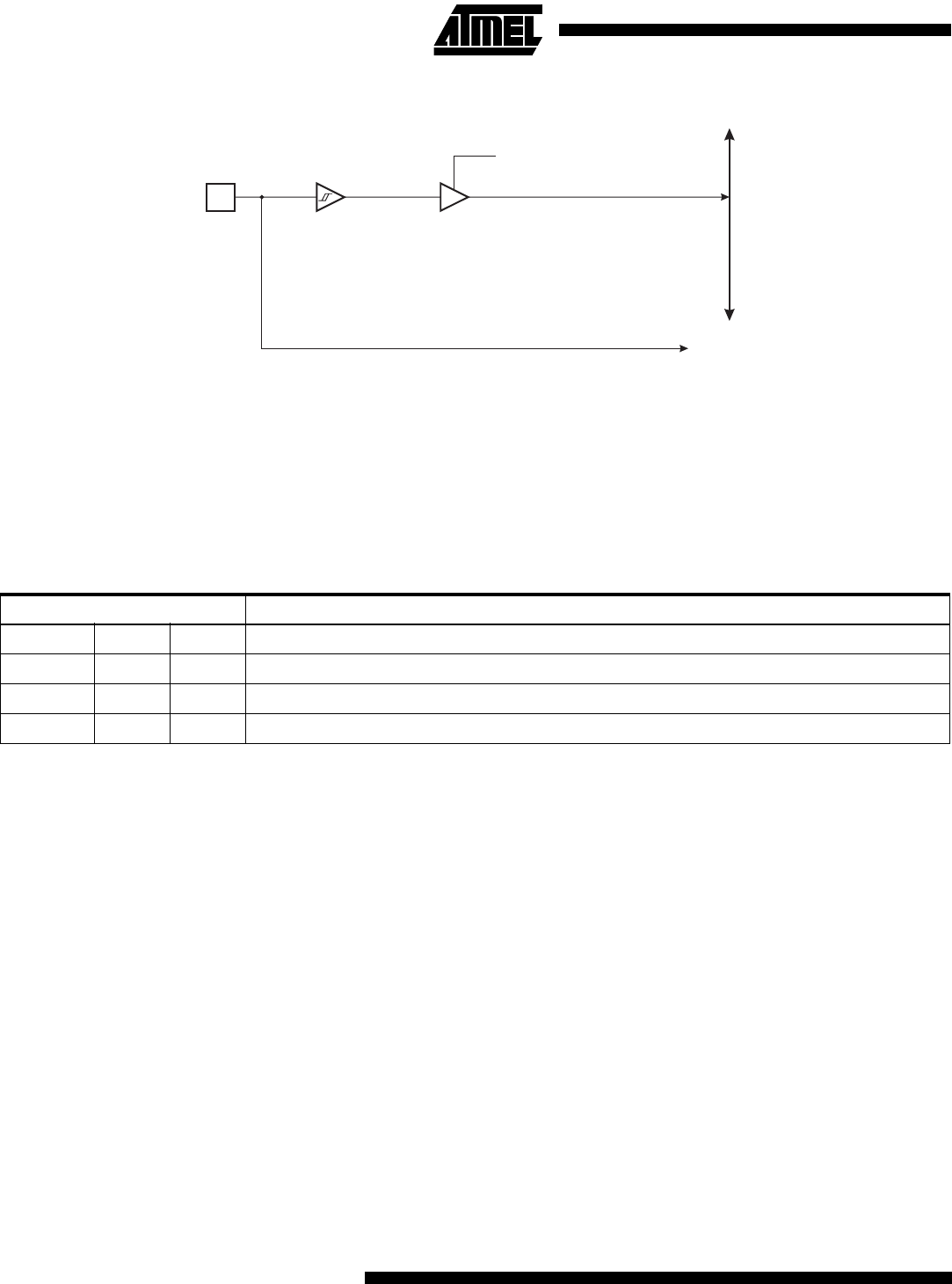
Figure 71. Port F Schematic Diagram (Pins PF7 - PF0)
Memory Programming
Program and Data Memory Lock Bits
The ATmega603/103 MCU provides two Lock bits which can be left unprogrammed (‘1’) or can be programmed (‘0’) to
obtain the additional features listed in Table 36. The Lock bits can only be erased to ‘1’ with the Chip Erase command..
Note: 1. In Parallel mode, programming of the Fuse bits are also disabled. Program the Fuse bits before programming the Lock bits.
Fuse Bits
The ATmega603/103 has four Fuse bits, SPIEN, SUT1..0, and EESAVE.
• When the SPIEN Fuse is programmed (‘0’), Serial Program and Data Downloading is enabled. Default value is
programmed (‘0’). The SPIEN Fuse is not accessible in serial programming mode.
• When EESAVE is programmed, the EEPROM memory is preserved through the Chip Erase cycle. Default value is
unprogrammed (‘1’). The EESAVE Fuse bit can not be programmed if any of the Lock bits are programmed.
• SUT1..0 Fuses: Determine the MCU start-up time. See Table 6 on page 26 for further details. Default value is un-
programmed (‘11’), which gives a nominal start up time of 16 ms.
The status of the Fuse bits is not affected by Chip Erase.
Table 36. Lock Bit Protection Modes
Memory Lock Bits Protection Type
Mode LB1 LB2
1 1 1 No memory lock features enabled.
2 0 1 Further programming of the Flash and EEPROM is disabled.
(1)
3 0 0 Same as mode 2, and verify is also disabled.
DATA B
US
PFn
AINn
TO ADC MUX
RP:
n:
READ PORTF PIN
0 - 7
RP