
Manual


Table Of Contents
- Ordering Information
- Features
- Description
- Architectural Overview
- General Purpose Register File
- ALU - Arithmetic Logic Unit
- ISP Flash Program Memory
- SRAM Data Memory
- Program and Data Addressing Modes
- Register Direct, Single Register Rd
- Register Direct, Two Registers Rd and Rr
- I/O Direct
- Data Direct
- Data Indirect with Displacement
- Data Indirect
- Data Indirect With Pre-Decrement
- Data Indirect With Post-Increment
- Constant Addressing Using the LPM and ELPM Instructions
- Direct Program Address, JMP and CALL
- Indirect Program Addressing, IJMP and ICALL
- Relative Program Addressing, RJMP and RCALL
- EEPROM Data Memory
- Memory Access Times and Instruction Execution Timing
- I/O Memory
- Reset and Interrupt Handling
- Reset Sources
- Power-On Reset
- External Reset
- Watchdog Reset
- MCU Status Register - MCUSR
- Interrupt Handling
- External Interrupt Mask Register - EIMSK
- External Interrupt Flag Register - EIFR
- External Interrupt Control Register - EICR
- Timer/Counter Interrupt Mask Register - TIMSK
- Timer/Counter Interrupt Flag Register - TIFR
- Interrupt Response Time
- Sleep Modes
- Timer/Counters
- Timer/Counter Prescalers
- 8-bit Timer/Counters T/C0 and T/C2
- Timer/Counter0 Control Register - TCCR0
- Timer/Counter2 Control Register - TCCR2
- Timer/Counter0 - TCNT0
- Timer/Counter2 - TCNT2
- Timer/Counter0 Output Compare Register - OCR0
- Timer/Counter2 Output Compare Register - OCR2
- Timer/Counter 0 and 2 in PWM mode
- Asynchronous Status Register - ASSR
- Asynchronous Operation of Timer/Counter0
- 16-bit Timer/Counter1
- Timer/Counter1 Control Register A - TCCR1A
- Timer/Counter1 Control Register B - TCCR1B
- Timer/Counter1 - TCNT1H and TCNT1L
- Timer/Counter1 Output Compare Register - OCR1AH and OCR1AL
- Timer/Counter1 Output Compare Register - OCR1BH and OCR1BL
- Timer/Counter1 Input Capture Register - ICR1H and ICR1L
- Timer/Counter1 in PWM mode
- Watchdog Timer
- EEPROM Read/Write Access
- Serial Peripheral Interface - SPI
- UART
- Analog Comparator
- Analog to Digital Converter
- Interface to external SRAM
- I/O-Ports
- Memory Programming
- Electrical Characteristics
- Typical characteristics
- Register Summary
- Instruction Set Summary (Continued)
ATmega603/103
9
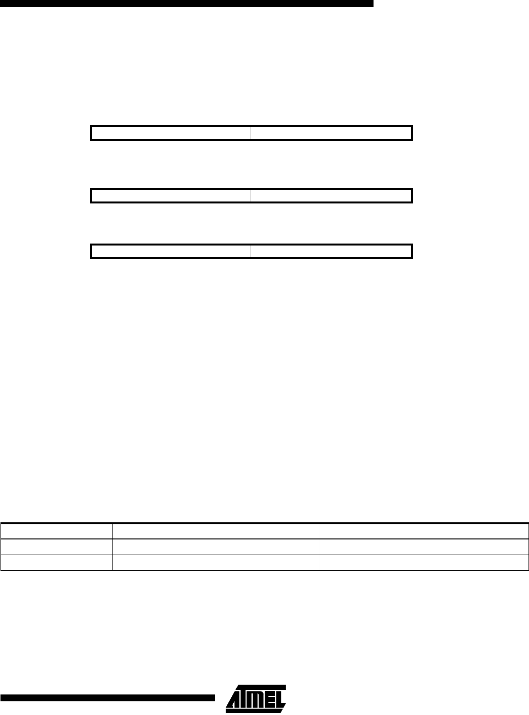
X-register, Y-register and Z-register
The registers R26..R31 have some added functions to their general purpose usage. These registers are address pointers
for indirect addressing of the SRAM. The three indirect address registers X, Y and Z are defined as:
Figure 6. X, Y and Z Registers
In the different addressing modes these address registers have functions as fixed displacement, automatic increment and
decrement (see the descriptions for the different instructions).
ALU - Arithmetic Logic Unit
The high-performance AVR ALU operates in direct connection with all the 32 general purpose working registers. Within a
single clock cycle, ALU operations between registers in the register file are executed. The ALU operations are divided into
three main categories - arithmetic, logical and bit-functions.
ISP Flash Program Memory
The ATmega603/103 contains 64K/128K bytes on-chip In-system Programmable Flash memory for program storage.
Since all instructions are single or double 16-bit words, the Flash is organized as 64K x 16. The Flash memory has an
endurance of at least 1000 write/erase cycles.
Constant tables can be allocated in the entire program memory space (see the LPM - Load Program Memory and ELPM
Extended Load Program Memory instruction descriptions).
SRAM Data Memory
The ATmega603/103 supports two different configurations for the SRAM data memory as listed in the following table:
Note: When using 64K of External SRAM, 60K will be available.
15 0
X - register 7 0 7 0
R27 ($1B) R26 ($1A)
15 0
Y - register 7 0 7 0
R29 ($1D) R28 ($1C)
15 0
Z - register 7 0 7 0
R31 ($1F) R30 ($1E)
Table 2. Memory Configurations
Configuration Internal SRAM Data Memory External SRAM Data Memory
A 4000 None
B 4000 up to 64K