
Manual


Table Of Contents
- Ordering Information
- Features
- Description
- Architectural Overview
- General Purpose Register File
- ALU - Arithmetic Logic Unit
- ISP Flash Program Memory
- SRAM Data Memory
- Program and Data Addressing Modes
- Register Direct, Single Register Rd
- Register Direct, Two Registers Rd and Rr
- I/O Direct
- Data Direct
- Data Indirect with Displacement
- Data Indirect
- Data Indirect With Pre-Decrement
- Data Indirect With Post-Increment
- Constant Addressing Using the LPM and ELPM Instructions
- Direct Program Address, JMP and CALL
- Indirect Program Addressing, IJMP and ICALL
- Relative Program Addressing, RJMP and RCALL
- EEPROM Data Memory
- Memory Access Times and Instruction Execution Timing
- I/O Memory
- Reset and Interrupt Handling
- Reset Sources
- Power-On Reset
- External Reset
- Watchdog Reset
- MCU Status Register - MCUSR
- Interrupt Handling
- External Interrupt Mask Register - EIMSK
- External Interrupt Flag Register - EIFR
- External Interrupt Control Register - EICR
- Timer/Counter Interrupt Mask Register - TIMSK
- Timer/Counter Interrupt Flag Register - TIFR
- Interrupt Response Time
- Sleep Modes
- Timer/Counters
- Timer/Counter Prescalers
- 8-bit Timer/Counters T/C0 and T/C2
- Timer/Counter0 Control Register - TCCR0
- Timer/Counter2 Control Register - TCCR2
- Timer/Counter0 - TCNT0
- Timer/Counter2 - TCNT2
- Timer/Counter0 Output Compare Register - OCR0
- Timer/Counter2 Output Compare Register - OCR2
- Timer/Counter 0 and 2 in PWM mode
- Asynchronous Status Register - ASSR
- Asynchronous Operation of Timer/Counter0
- 16-bit Timer/Counter1
- Timer/Counter1 Control Register A - TCCR1A
- Timer/Counter1 Control Register B - TCCR1B
- Timer/Counter1 - TCNT1H and TCNT1L
- Timer/Counter1 Output Compare Register - OCR1AH and OCR1AL
- Timer/Counter1 Output Compare Register - OCR1BH and OCR1BL
- Timer/Counter1 Input Capture Register - ICR1H and ICR1L
- Timer/Counter1 in PWM mode
- Watchdog Timer
- EEPROM Read/Write Access
- Serial Peripheral Interface - SPI
- UART
- Analog Comparator
- Analog to Digital Converter
- Interface to external SRAM
- I/O-Ports
- Memory Programming
- Electrical Characteristics
- Typical characteristics
- Register Summary
- Instruction Set Summary (Continued)
ATmega603/103
88
Port E as general digital I/O
PEn, General I/O pin: The DDEn bit in the DDRE register selects the direction of this pin. If DDEn is set (one), PEn is con-
figured as an output pin. If DDEn is cleared (zero), PEn is configured as an input pin. If PEn is set (one) when configured as
an input pin, the MOS pull up resistor is activated. To switch the pull up resistor off the PEn has to be cleared (zero) or the
pin has to be configured as an output pin.The port pins are tri-stated when a reset condition becomes active, even if the
clock is not running.
Note: n: 7,6...0, pin number
Alternate Functions OF Port E
PDI/RXD - Port E, Bit 0
PDI, Serial Programming Data Input. During Serial Program Downloading, this pin is used as data input line for the
ATmega603/103.
RXD, UART Receive Pin. Receive Data (Data input pin for the UART). When the UART receiver is enabled this pin is con-
figured as an input regardless of the value of DDRD0. When the UART forces this pin to be an input, a logical one in
PORTD0 will turn on the internal pull-up.
PDO/TXD - Port E, Bit 1
PDO, Serial Programming Data Output. During Serial Program Downloading, this pin is used as data output line for the
ATmega603/103.
TXD, UART Transmit Pin.
AC+ - Port E, Bit 2
AC+ - Analog Comparator Positive Input. This pin is directly connected to the positive input of the analog comparator.
AC- - Port E, Bit 3
AC- - Analog Comparator Negative Input. This pin is directly connected to the negative input of the analog comparator.
INT4 .. INT7 - Port E, Bit 4-7
INT4 .. INT7 - External Interrupt sources 4 - 7: The PE4 - PE7 pins can serve as external interrupt sources to the MCU.
Interrupts can be triggered by low level or positive or negative edge on these pins. The internal pull up MOS resistors can
be activated as described above. See the interrupt description for further details, and how to enable the sources.
Port E Schematics
Note that all port pins are synchronized. The synchronization latches are however, not shown in the figures.
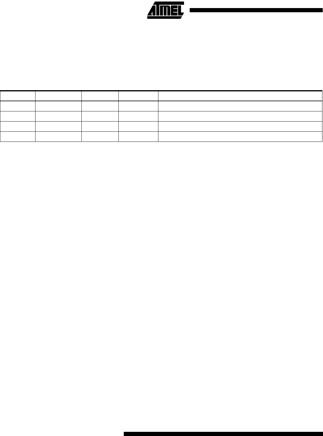
Table 35. DDEn Bits on Port E Pins
DDEn PORTEn I/O Pull up Comment
0 0 Input No Tri-state (Hi-Z)
0 1 Input Yes PDn will source current if ext. pulled low.
1 0 Output No Push-Pull Zero Output
1 1 Output No Push-Pull One Output