
Manual


Table Of Contents
- Ordering Information
- Features
- Description
- Architectural Overview
- General Purpose Register File
- ALU - Arithmetic Logic Unit
- ISP Flash Program Memory
- SRAM Data Memory
- Program and Data Addressing Modes
- Register Direct, Single Register Rd
- Register Direct, Two Registers Rd and Rr
- I/O Direct
- Data Direct
- Data Indirect with Displacement
- Data Indirect
- Data Indirect With Pre-Decrement
- Data Indirect With Post-Increment
- Constant Addressing Using the LPM and ELPM Instructions
- Direct Program Address, JMP and CALL
- Indirect Program Addressing, IJMP and ICALL
- Relative Program Addressing, RJMP and RCALL
- EEPROM Data Memory
- Memory Access Times and Instruction Execution Timing
- I/O Memory
- Reset and Interrupt Handling
- Reset Sources
- Power-On Reset
- External Reset
- Watchdog Reset
- MCU Status Register - MCUSR
- Interrupt Handling
- External Interrupt Mask Register - EIMSK
- External Interrupt Flag Register - EIFR
- External Interrupt Control Register - EICR
- Timer/Counter Interrupt Mask Register - TIMSK
- Timer/Counter Interrupt Flag Register - TIFR
- Interrupt Response Time
- Sleep Modes
- Timer/Counters
- Timer/Counter Prescalers
- 8-bit Timer/Counters T/C0 and T/C2
- Timer/Counter0 Control Register - TCCR0
- Timer/Counter2 Control Register - TCCR2
- Timer/Counter0 - TCNT0
- Timer/Counter2 - TCNT2
- Timer/Counter0 Output Compare Register - OCR0
- Timer/Counter2 Output Compare Register - OCR2
- Timer/Counter 0 and 2 in PWM mode
- Asynchronous Status Register - ASSR
- Asynchronous Operation of Timer/Counter0
- 16-bit Timer/Counter1
- Timer/Counter1 Control Register A - TCCR1A
- Timer/Counter1 Control Register B - TCCR1B
- Timer/Counter1 - TCNT1H and TCNT1L
- Timer/Counter1 Output Compare Register - OCR1AH and OCR1AL
- Timer/Counter1 Output Compare Register - OCR1BH and OCR1BL
- Timer/Counter1 Input Capture Register - ICR1H and ICR1L
- Timer/Counter1 in PWM mode
- Watchdog Timer
- EEPROM Read/Write Access
- Serial Peripheral Interface - SPI
- UART
- Analog Comparator
- Analog to Digital Converter
- Interface to external SRAM
- I/O-Ports
- Memory Programming
- Electrical Characteristics
- Typical characteristics
- Register Summary
- Instruction Set Summary (Continued)
ATmega603/103
87
Port E
Port E is an 8-bit bi-directional I/O port with internal pull-up resistors.
Three I/O memory address locations are allocated for the Port E, one each for the Data Register - PORTE, $03($23), Data
Direction Register - DDRE, $02($22) and the Port E Input Pins - PINE, $01($21). The Port E Input Pins address is read
only, while the Data Register and the Data Direction Register are read/write.
The Port E output buffers can sink 20 mA. As inputs, Port E pins that are externally pulled low will source current if the pull-
up resistors are activated.
All Port E pins have alternate functions as shown in the following table:
When the pins are used for the alternate function the DDRE and PORTE register has to be set according to the alternate
function description.
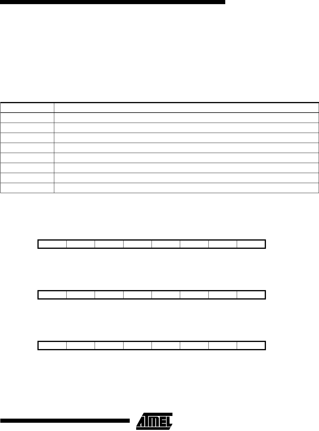
Port E Data Register - PORTE
Port E Data Direction Register - DDRE
Port E Input Pins Address - PINE
The Port E Input Pins address - PINE - is not a register, and this address enables access to the physical value on each Port
E pin. When reading PORTE, the Port E Data Latch is read, and when reading PINE, the logical values present on the pins
are read.
Table 34. Port E Pins Alternate Functions
Port Pin Alternate Function
PE0 PDI/RXD (Programming Data Input or UART Receive Pin)
PE1 PDO/TXD (Programming Data Output or UART Transmit Pin)
PE2 AC+ (Analog Comparator Positive Input)
PE3 AC- (Analog Comparator Negative Input)
PE4 INT4 (External Interrupt4 Input)
PE5 INT5 (External Interrupt5 Input)
PE6 INT6 (External Interrupt6 Input)
PE7 INT7 (External Interrupt7 Input)
Bit 76543210
$03 ($23) PORTE7 PORTE6 PORTE5 PORTE4 PORTE3 PORTE2 PORTE1 PORTE0 PORTE
Read/Write R/W R/W R/W R/W R/W R/W R/W R/W
Initial value00000000
Bit 76543210
$02 ($22) DDE7 DDE6 DDE5 DDE4 DDE3 DDE2 DDE1 DDE0 DDRE
Read/Write R/W R/W R/W R/W R/W R/W R/W R/W
Initial value00000000
Bit 76543210
$01 ($21) PINE7 PINE6 PINE5 PINE4 PINE3 PINE2 PINE1 PINE0 PINE
Read/WriteRRRRRRRR
Initial value Hi-Z Hi-Z Hi-Z Hi-Z Hi-Z Hi-Z Hi-Z Hi-Z