
Manual


Table Of Contents
- Ordering Information
- Features
- Description
- Architectural Overview
- General Purpose Register File
- ALU - Arithmetic Logic Unit
- ISP Flash Program Memory
- SRAM Data Memory
- Program and Data Addressing Modes
- Register Direct, Single Register Rd
- Register Direct, Two Registers Rd and Rr
- I/O Direct
- Data Direct
- Data Indirect with Displacement
- Data Indirect
- Data Indirect With Pre-Decrement
- Data Indirect With Post-Increment
- Constant Addressing Using the LPM and ELPM Instructions
- Direct Program Address, JMP and CALL
- Indirect Program Addressing, IJMP and ICALL
- Relative Program Addressing, RJMP and RCALL
- EEPROM Data Memory
- Memory Access Times and Instruction Execution Timing
- I/O Memory
- Reset and Interrupt Handling
- Reset Sources
- Power-On Reset
- External Reset
- Watchdog Reset
- MCU Status Register - MCUSR
- Interrupt Handling
- External Interrupt Mask Register - EIMSK
- External Interrupt Flag Register - EIFR
- External Interrupt Control Register - EICR
- Timer/Counter Interrupt Mask Register - TIMSK
- Timer/Counter Interrupt Flag Register - TIFR
- Interrupt Response Time
- Sleep Modes
- Timer/Counters
- Timer/Counter Prescalers
- 8-bit Timer/Counters T/C0 and T/C2
- Timer/Counter0 Control Register - TCCR0
- Timer/Counter2 Control Register - TCCR2
- Timer/Counter0 - TCNT0
- Timer/Counter2 - TCNT2
- Timer/Counter0 Output Compare Register - OCR0
- Timer/Counter2 Output Compare Register - OCR2
- Timer/Counter 0 and 2 in PWM mode
- Asynchronous Status Register - ASSR
- Asynchronous Operation of Timer/Counter0
- 16-bit Timer/Counter1
- Timer/Counter1 Control Register A - TCCR1A
- Timer/Counter1 Control Register B - TCCR1B
- Timer/Counter1 - TCNT1H and TCNT1L
- Timer/Counter1 Output Compare Register - OCR1AH and OCR1AL
- Timer/Counter1 Output Compare Register - OCR1BH and OCR1BL
- Timer/Counter1 Input Capture Register - ICR1H and ICR1L
- Timer/Counter1 in PWM mode
- Watchdog Timer
- EEPROM Read/Write Access
- Serial Peripheral Interface - SPI
- UART
- Analog Comparator
- Analog to Digital Converter
- Interface to external SRAM
- I/O-Ports
- Memory Programming
- Electrical Characteristics
- Typical characteristics
- Register Summary
- Instruction Set Summary (Continued)
ATmega603/103
83
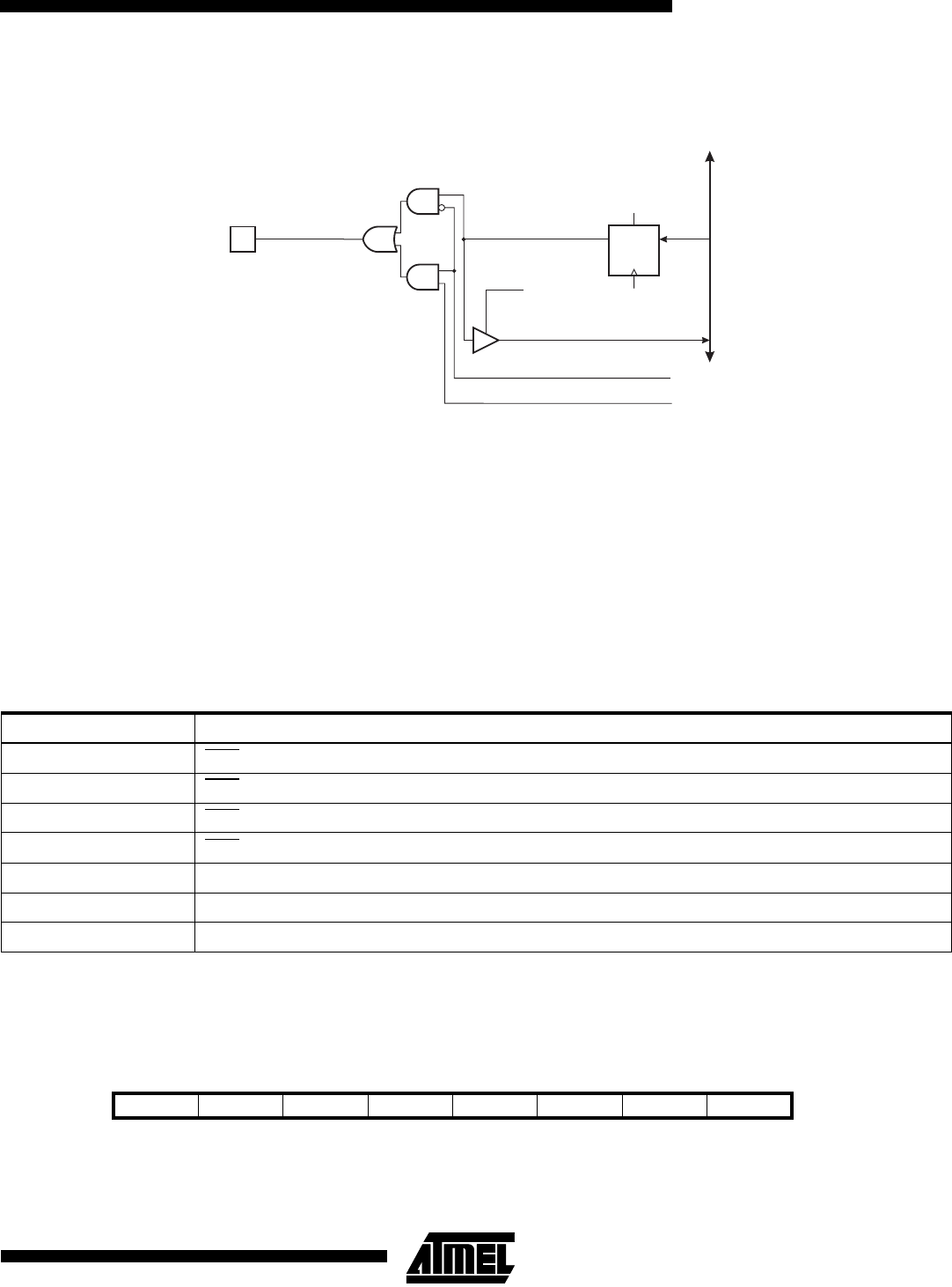
Port C Schematics
Figure 61. Port C Schematic Diagram (Pins PC0 - PC7)
Port D
Port D is an 8 bit bi-directional I/O port with internal pull-up resistors.
Three I/O memory address locations are allocated for the Port D, one each for the Data Register - PORTD, $12($32), Data
Direction Register - DDRD, $11($31) and the Port D Input Pins - PIND, $10($30). The Port D Input Pins address is read
only, while the Data Register and the Data Direction Register are read/write.
The Port D output buffers can sink 20 mA. As inputs, Port D pins that are externally pulled low will source current if the pull-
up resistors are activated.
Some Port D pins have alternate functions as shown in the following table:
When the pins are used for the alternate function the DDRD and PORTD register has to be set according to the alternate
function description.
Port D Data Register - PORTD
Table 32. Port D Pins Alternate Functions
Port Pin Alternate Function
PD0 INT0 (External Interrupt0 Input)
PD1 INT1
(External Interrupt1 Input)
PD2 INT2
(External Interrupt2 Input)
PD3 INT3 (External Interrupt3 Input)
PD4 IC1 (Timer/Counter1 Input Capture Trigger)
PD6 T1 (Timer/Counter1 Clock Input)
PD7 T2 (Timer/Counter2 Clock Input)
Bit 76543210
$12 PORTD7 PORTD6 PORTD5 PORTD4 PORTD3 PORTD2 PORTD1 PORTD0 PORTD
Read/Write R/W R/W R/W R/W R/W R/W R/W R/W
Initial value00000000
DATA B
US
D
Q
RESET
C
WP
PCn
R
WP:
RL:
A:
SRE:
n:
WRITE PORTC
READ PORTC LATCH
SRAM ADDRESS
EXTERNAL SRAM ENABLE
0-7
PORTCn
SRE
An
RL