
Manual


Table Of Contents
- Ordering Information
- Features
- Description
- Architectural Overview
- General Purpose Register File
- ALU - Arithmetic Logic Unit
- ISP Flash Program Memory
- SRAM Data Memory
- Program and Data Addressing Modes
- Register Direct, Single Register Rd
- Register Direct, Two Registers Rd and Rr
- I/O Direct
- Data Direct
- Data Indirect with Displacement
- Data Indirect
- Data Indirect With Pre-Decrement
- Data Indirect With Post-Increment
- Constant Addressing Using the LPM and ELPM Instructions
- Direct Program Address, JMP and CALL
- Indirect Program Addressing, IJMP and ICALL
- Relative Program Addressing, RJMP and RCALL
- EEPROM Data Memory
- Memory Access Times and Instruction Execution Timing
- I/O Memory
- Reset and Interrupt Handling
- Reset Sources
- Power-On Reset
- External Reset
- Watchdog Reset
- MCU Status Register - MCUSR
- Interrupt Handling
- External Interrupt Mask Register - EIMSK
- External Interrupt Flag Register - EIFR
- External Interrupt Control Register - EICR
- Timer/Counter Interrupt Mask Register - TIMSK
- Timer/Counter Interrupt Flag Register - TIFR
- Interrupt Response Time
- Sleep Modes
- Timer/Counters
- Timer/Counter Prescalers
- 8-bit Timer/Counters T/C0 and T/C2
- Timer/Counter0 Control Register - TCCR0
- Timer/Counter2 Control Register - TCCR2
- Timer/Counter0 - TCNT0
- Timer/Counter2 - TCNT2
- Timer/Counter0 Output Compare Register - OCR0
- Timer/Counter2 Output Compare Register - OCR2
- Timer/Counter 0 and 2 in PWM mode
- Asynchronous Status Register - ASSR
- Asynchronous Operation of Timer/Counter0
- 16-bit Timer/Counter1
- Timer/Counter1 Control Register A - TCCR1A
- Timer/Counter1 Control Register B - TCCR1B
- Timer/Counter1 - TCNT1H and TCNT1L
- Timer/Counter1 Output Compare Register - OCR1AH and OCR1AL
- Timer/Counter1 Output Compare Register - OCR1BH and OCR1BL
- Timer/Counter1 Input Capture Register - ICR1H and ICR1L
- Timer/Counter1 in PWM mode
- Watchdog Timer
- EEPROM Read/Write Access
- Serial Peripheral Interface - SPI
- UART
- Analog Comparator
- Analog to Digital Converter
- Interface to external SRAM
- I/O-Ports
- Memory Programming
- Electrical Characteristics
- Typical characteristics
- Register Summary
- Instruction Set Summary (Continued)
ATmega603/103
74
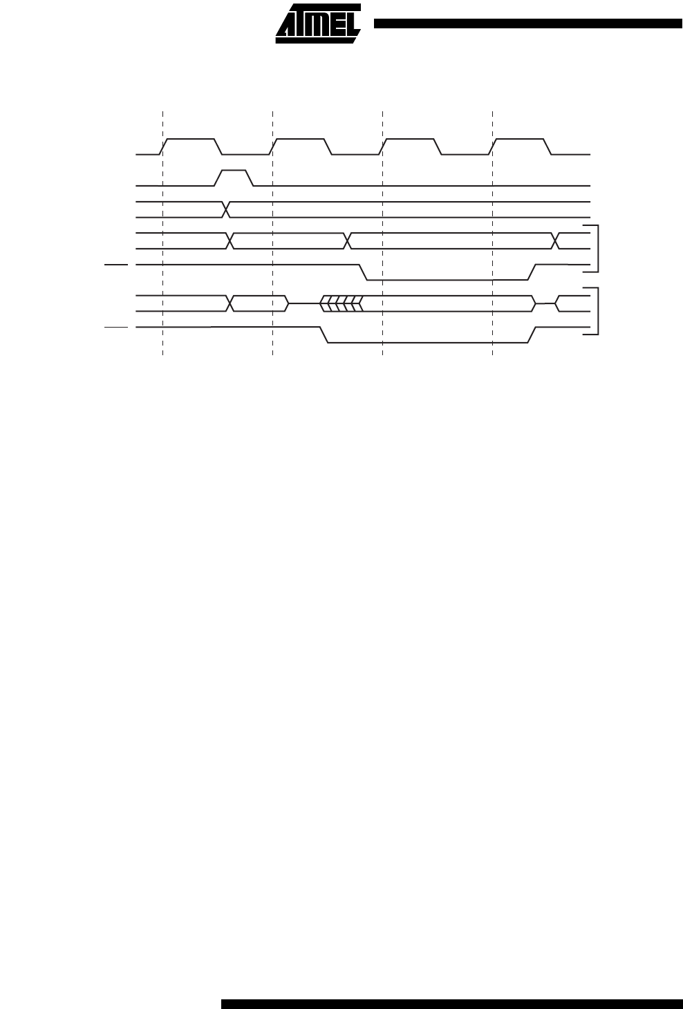
Figure 52. External SRAM Access Cycle with wait state
I/O-Ports
All AVR ports have true Read-Modify-Write functionality when used as general digital I/O ports. This means that the direc-
tion of one port pin can be changed without unintentionally changing the direction of any other pin with the SBI and CBI
instructions. The same applies for changing drive value (if configured as output) or enabling/disabling of pull-up resistors (if
configured as input).
Port A
Port A is an 8-bit bi-directional I/O port with internal pull-ups.
Three I/O memory address locations are allocated for Port A, one each for the Data Register - PORTA, $1B($3B), Data
Direction Register - DDRA, $1A($3A) and the Port A Input Pins - PINA, $19($39). The Port A Input Pins address is read
only, while the Data Register and the Data Direction Register are read/write.
All port pins have individually selectable pull-up resistors. The Port A output buffers can sink 20mA and thus drive LED
displays directly. When pins PA0 to PA7 are used as inputs and are externally pulled low, they will source current if the
internal pull-up resistors are activated.
The Port A pins have alternate functions related to the optional external data SRAM. Port A can be configured to be the
multiplexed low-order address/data bus during accesses to the byte.
When Port A is set to the alternate function by the SRE - External SRAM Enable - bit in the MCUCR - MCU Control Regis-
ter, the alternate settings override the data direction register.
System Clock Ø
ALE
WR
RD
Data / Address [7..0]
Data / Address [7..0]
Address [15..8]
Address
Address
Address
T1 T2 T3 T4
Prev. Address
Prev. Address
Prev. Address
Data
Data
WriteRead
Addr.
Addr.