
Manual


Table Of Contents
- Ordering Information
- Features
- Description
- Architectural Overview
- General Purpose Register File
- ALU - Arithmetic Logic Unit
- ISP Flash Program Memory
- SRAM Data Memory
- Program and Data Addressing Modes
- Register Direct, Single Register Rd
- Register Direct, Two Registers Rd and Rr
- I/O Direct
- Data Direct
- Data Indirect with Displacement
- Data Indirect
- Data Indirect With Pre-Decrement
- Data Indirect With Post-Increment
- Constant Addressing Using the LPM and ELPM Instructions
- Direct Program Address, JMP and CALL
- Indirect Program Addressing, IJMP and ICALL
- Relative Program Addressing, RJMP and RCALL
- EEPROM Data Memory
- Memory Access Times and Instruction Execution Timing
- I/O Memory
- Reset and Interrupt Handling
- Reset Sources
- Power-On Reset
- External Reset
- Watchdog Reset
- MCU Status Register - MCUSR
- Interrupt Handling
- External Interrupt Mask Register - EIMSK
- External Interrupt Flag Register - EIFR
- External Interrupt Control Register - EICR
- Timer/Counter Interrupt Mask Register - TIMSK
- Timer/Counter Interrupt Flag Register - TIFR
- Interrupt Response Time
- Sleep Modes
- Timer/Counters
- Timer/Counter Prescalers
- 8-bit Timer/Counters T/C0 and T/C2
- Timer/Counter0 Control Register - TCCR0
- Timer/Counter2 Control Register - TCCR2
- Timer/Counter0 - TCNT0
- Timer/Counter2 - TCNT2
- Timer/Counter0 Output Compare Register - OCR0
- Timer/Counter2 Output Compare Register - OCR2
- Timer/Counter 0 and 2 in PWM mode
- Asynchronous Status Register - ASSR
- Asynchronous Operation of Timer/Counter0
- 16-bit Timer/Counter1
- Timer/Counter1 Control Register A - TCCR1A
- Timer/Counter1 Control Register B - TCCR1B
- Timer/Counter1 - TCNT1H and TCNT1L
- Timer/Counter1 Output Compare Register - OCR1AH and OCR1AL
- Timer/Counter1 Output Compare Register - OCR1BH and OCR1BL
- Timer/Counter1 Input Capture Register - ICR1H and ICR1L
- Timer/Counter1 in PWM mode
- Watchdog Timer
- EEPROM Read/Write Access
- Serial Peripheral Interface - SPI
- UART
- Analog Comparator
- Analog to Digital Converter
- Interface to external SRAM
- I/O-Ports
- Memory Programming
- Electrical Characteristics
- Typical characteristics
- Register Summary
- Instruction Set Summary (Continued)
ATmega603/103
72
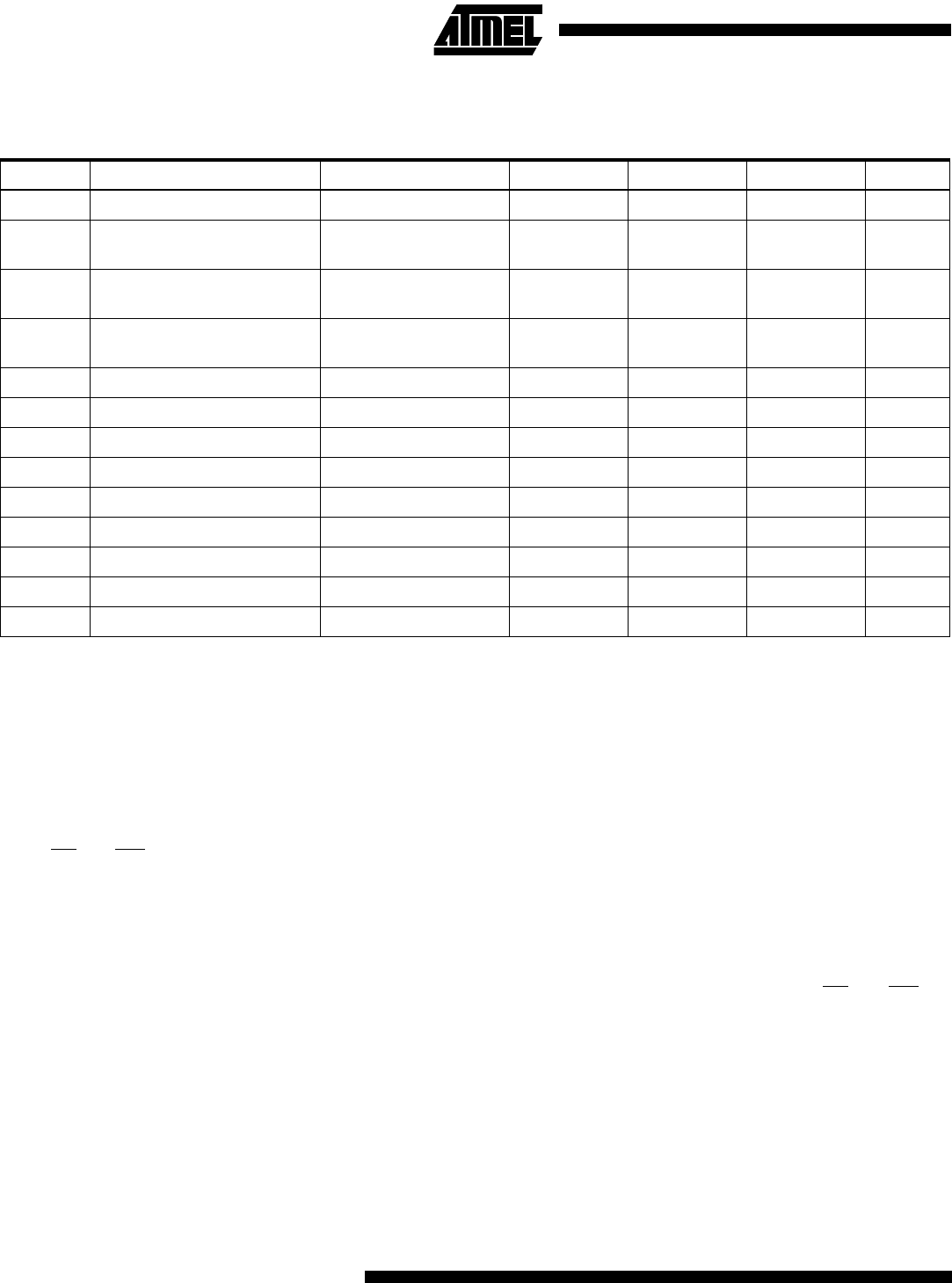
ADC DC Characteristics
Notes: 1. Minimum for AV
CC
is 2.7V.
2. Maximum for AV
CC
is 6.0V.
Interface to external SRAM
The interface to the SRAM consists of:
• Port A: Multiplexed low-order address bus and data bus
• Port C: High-order address bus
• The ALE-pin: Address latch enable
• The RD
and WR-pin: Read and write strobes.
The external data SRAM is enabled by setting the SRE - External SRAM enable bit of the MCUCR - MCU control register,
and will override the setting of the data direction register DDRA. When the SRE bit is cleared (zero), the external data
SRAM is disabled, and the normal pin and data direction settings are used. When SRE is cleared (zero), the address space
above the internal SRAM boundary is not mapped into the internal SRAM, as in AVR parts not having interface to the
external SRAM.
When ALE goes from high to low, there is a valid address on Port A. ALE is low during a data transfer. RD
and WR are
active when accessing the external SRAM only.
When the external SRAM is enabled, the ALE signal may have short pulses when accessing the internal RAM, but the ALE
signal is stable when accessing the external SRAM.
Figure 50 sketches how to connect an external SRAM to the AVR using 8 latches which are transparent when G is high.
Default, the external SRAM access is a three-cycle scheme as depicted in Figure 51. When one extra wait state is needed
in the access cycle, set the SRW bit (one) in the MCUCR register. The resulting access scheme is shown in Figure 52. In
both cases, note that Port A is data bus in one cycle only. As soon as the data access finishes, Port A becomes a low order
address bus again.
TA=-40°C to 85°C
Symbol Parameter Condition Min Typ Max Units
Resolution 10 Bits
Absolute accuracy
VREF = 4V, V
CC
= 4V
ADC clock = 200 kHz
12LSB
Absolute accuracy
VREF = 4V, V
CC
= 4V
ADC clock = 1 MHz
4LSB
Absolute accuracy
VREF = 4V, V
CC
= 4V
ADC clock = 2 MHz
16 LSB
Integral Non-Linearity VREF > 2V 0.5 LSB
Differential Non-Linearity VREF > 2V 0.5 LSB
Zero Error (Offset) 1 LSB
Conversion Time 70 280
µs
Clock Frequency 50 200 kHz
AV
CC
Analog Supply Voltage V
CC
–0.3
(1)
V
CC
+0.3
(2)
V
V
REF
Reference Voltage AGND AV
CC
V
R
REF
Reference Input Resistance 6 10 13 kΩ
R
AIN
Analog Input Resistance 100 MΩ