
Manual


Table Of Contents
- Ordering Information
- Features
- Description
- Architectural Overview
- General Purpose Register File
- ALU - Arithmetic Logic Unit
- ISP Flash Program Memory
- SRAM Data Memory
- Program and Data Addressing Modes
- Register Direct, Single Register Rd
- Register Direct, Two Registers Rd and Rr
- I/O Direct
- Data Direct
- Data Indirect with Displacement
- Data Indirect
- Data Indirect With Pre-Decrement
- Data Indirect With Post-Increment
- Constant Addressing Using the LPM and ELPM Instructions
- Direct Program Address, JMP and CALL
- Indirect Program Addressing, IJMP and ICALL
- Relative Program Addressing, RJMP and RCALL
- EEPROM Data Memory
- Memory Access Times and Instruction Execution Timing
- I/O Memory
- Reset and Interrupt Handling
- Reset Sources
- Power-On Reset
- External Reset
- Watchdog Reset
- MCU Status Register - MCUSR
- Interrupt Handling
- External Interrupt Mask Register - EIMSK
- External Interrupt Flag Register - EIFR
- External Interrupt Control Register - EICR
- Timer/Counter Interrupt Mask Register - TIMSK
- Timer/Counter Interrupt Flag Register - TIFR
- Interrupt Response Time
- Sleep Modes
- Timer/Counters
- Timer/Counter Prescalers
- 8-bit Timer/Counters T/C0 and T/C2
- Timer/Counter0 Control Register - TCCR0
- Timer/Counter2 Control Register - TCCR2
- Timer/Counter0 - TCNT0
- Timer/Counter2 - TCNT2
- Timer/Counter0 Output Compare Register - OCR0
- Timer/Counter2 Output Compare Register - OCR2
- Timer/Counter 0 and 2 in PWM mode
- Asynchronous Status Register - ASSR
- Asynchronous Operation of Timer/Counter0
- 16-bit Timer/Counter1
- Timer/Counter1 Control Register A - TCCR1A
- Timer/Counter1 Control Register B - TCCR1B
- Timer/Counter1 - TCNT1H and TCNT1L
- Timer/Counter1 Output Compare Register - OCR1AH and OCR1AL
- Timer/Counter1 Output Compare Register - OCR1BH and OCR1BL
- Timer/Counter1 Input Capture Register - ICR1H and ICR1L
- Timer/Counter1 in PWM mode
- Watchdog Timer
- EEPROM Read/Write Access
- Serial Peripheral Interface - SPI
- UART
- Analog Comparator
- Analog to Digital Converter
- Interface to external SRAM
- I/O-Ports
- Memory Programming
- Electrical Characteristics
- Typical characteristics
- Register Summary
- Instruction Set Summary (Continued)
ATmega603/103
71
ADC Data Register - ADCL and ADCH
When an ADC conversion is complete, the result is found in these two registers. It is essential that both registers are read,
and that ADCL is read before ADCH.
ADC Noise Canceling Techniques
Digital circuitry inside and outside the ATmega603/103 generates EMI which might affect the accuracy of analog measure-
ments. If conversion accuracy is critical, the noise level can be reduced by applying the following techniques:
1. The analog part of the ATmega603/103 and all analog components in the application should have a separate ana-
log ground plane on the PCB. This ground plane is connected to the digital ground plane via a single point on the
PCB.
2. Keep analog signal paths as short as possible. Make sure analog tracks run over the analog ground plane, and keep
them well away from high-speed switching digital tracks.
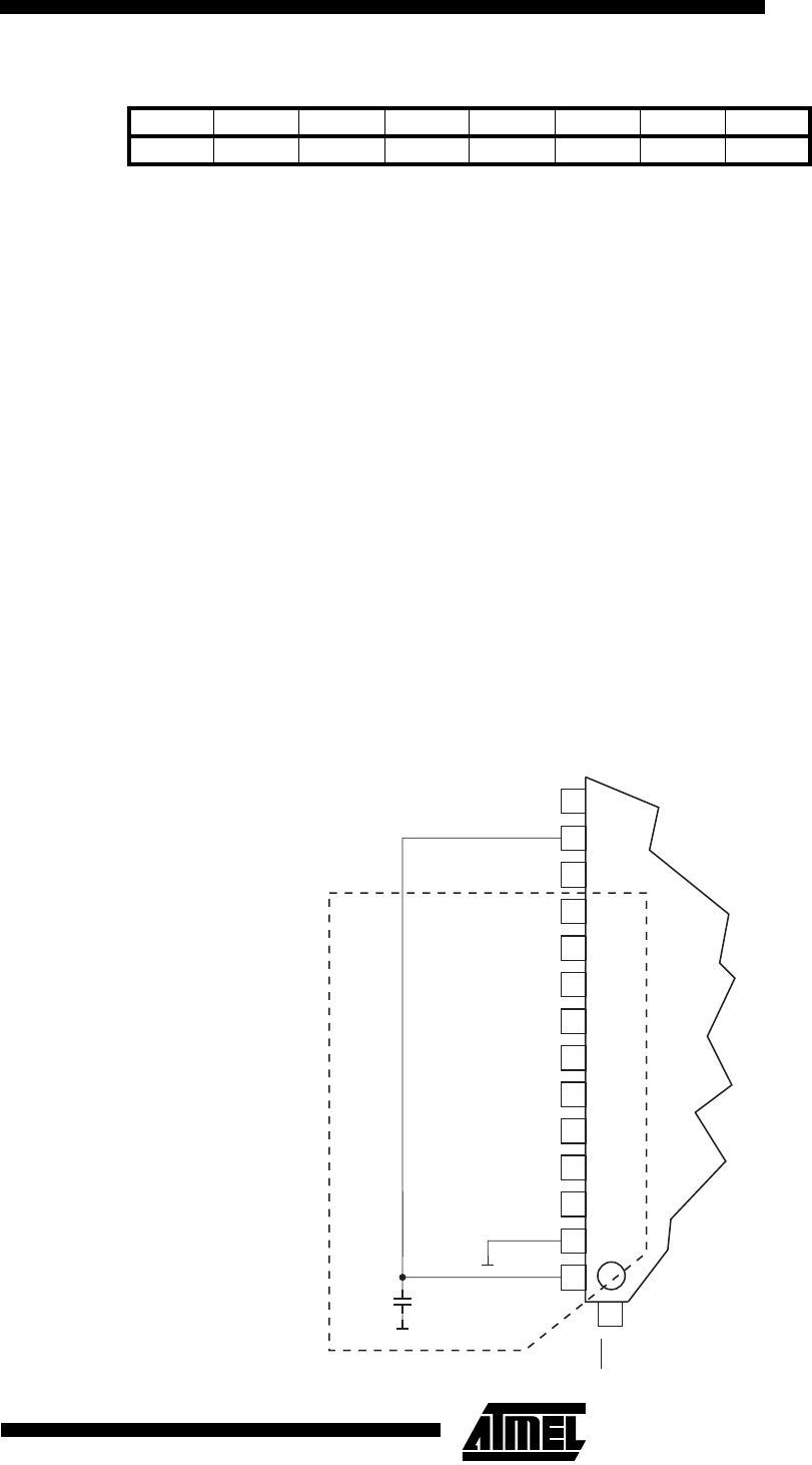
3. The AV
CC
pin on the ATmega603/103 should have its own decoupling capacitor as shown in Figure 49.
4. Use the ADC noise canceler function to reduce induced noise from the CPU.
5. If some Port F pins are used as digital inputs, it is essential that these do not switch while a conversion is in
progress.
Figure 49. ADC Power Connections
Bit 151413121110 9 8
$05 ($25) - - - - - - ADC9 ADC8 ADCH
$04 ($24) ADC7 ADC6 ADC5 ADC4 ADC3 ADC2 ADC1 ADC0 ADCL
76543210
Read/WriteRRRRRRRR
RRRRRRRR
Initial value00000000
00000000
VCC
GND
10nF
Analog Ground Plane
ATmega603/103
(ADC0) PF0
(ADC7) PF7
(ADC1) PF1
(ADC2) PF2
(ADC3) PF3
(ADC4) PF4
(ADC5) PF5
(ADC6) PF6
AREF
AGND
AVCC
52
53
54
55
56
57
58
59
60
6161
6262
6363
6464
1
51
PEN
(AD0) PA0