
Manual


Table Of Contents
- Ordering Information
- Features
- Description
- Architectural Overview
- General Purpose Register File
- ALU - Arithmetic Logic Unit
- ISP Flash Program Memory
- SRAM Data Memory
- Program and Data Addressing Modes
- Register Direct, Single Register Rd
- Register Direct, Two Registers Rd and Rr
- I/O Direct
- Data Direct
- Data Indirect with Displacement
- Data Indirect
- Data Indirect With Pre-Decrement
- Data Indirect With Post-Increment
- Constant Addressing Using the LPM and ELPM Instructions
- Direct Program Address, JMP and CALL
- Indirect Program Addressing, IJMP and ICALL
- Relative Program Addressing, RJMP and RCALL
- EEPROM Data Memory
- Memory Access Times and Instruction Execution Timing
- I/O Memory
- Reset and Interrupt Handling
- Reset Sources
- Power-On Reset
- External Reset
- Watchdog Reset
- MCU Status Register - MCUSR
- Interrupt Handling
- External Interrupt Mask Register - EIMSK
- External Interrupt Flag Register - EIFR
- External Interrupt Control Register - EICR
- Timer/Counter Interrupt Mask Register - TIMSK
- Timer/Counter Interrupt Flag Register - TIFR
- Interrupt Response Time
- Sleep Modes
- Timer/Counters
- Timer/Counter Prescalers
- 8-bit Timer/Counters T/C0 and T/C2
- Timer/Counter0 Control Register - TCCR0
- Timer/Counter2 Control Register - TCCR2
- Timer/Counter0 - TCNT0
- Timer/Counter2 - TCNT2
- Timer/Counter0 Output Compare Register - OCR0
- Timer/Counter2 Output Compare Register - OCR2
- Timer/Counter 0 and 2 in PWM mode
- Asynchronous Status Register - ASSR
- Asynchronous Operation of Timer/Counter0
- 16-bit Timer/Counter1
- Timer/Counter1 Control Register A - TCCR1A
- Timer/Counter1 Control Register B - TCCR1B
- Timer/Counter1 - TCNT1H and TCNT1L
- Timer/Counter1 Output Compare Register - OCR1AH and OCR1AL
- Timer/Counter1 Output Compare Register - OCR1BH and OCR1BL
- Timer/Counter1 Input Capture Register - ICR1H and ICR1L
- Timer/Counter1 in PWM mode
- Watchdog Timer
- EEPROM Read/Write Access
- Serial Peripheral Interface - SPI
- UART
- Analog Comparator
- Analog to Digital Converter
- Interface to external SRAM
- I/O-Ports
- Memory Programming
- Electrical Characteristics
- Typical characteristics
- Register Summary
- Instruction Set Summary (Continued)
ATmega603/103
64
•
Bit 0 - TXB8: Transmit Data Bit 8
When CHR9 is set (one), TXB8 is the 9th data bit in the character to be transmitted.
Baud Rate Generator
The baud rate generator is a frequency divider which generates baud rates according to the following equation:
• BAUD = Baud Rate
•f
CK
= CPU Clock frequency
• UBRR = Contents of the UART Baud Rate register, UBRR (0 - 255)
For standard crystal frequencies, the most commonly used baud rates can be generated by using the UBRR settings in
Table 25. Observe that CPU clock frequency can be lower than the XTAL frequency if the XTAL divider is enabled. UBRR
values which yield an actual baud rate differing less than 2% from the target baud rate, are bolded in the table. However,
using baud rates that have more than 1% error is not recommended. High error ratings give less noise resistance.
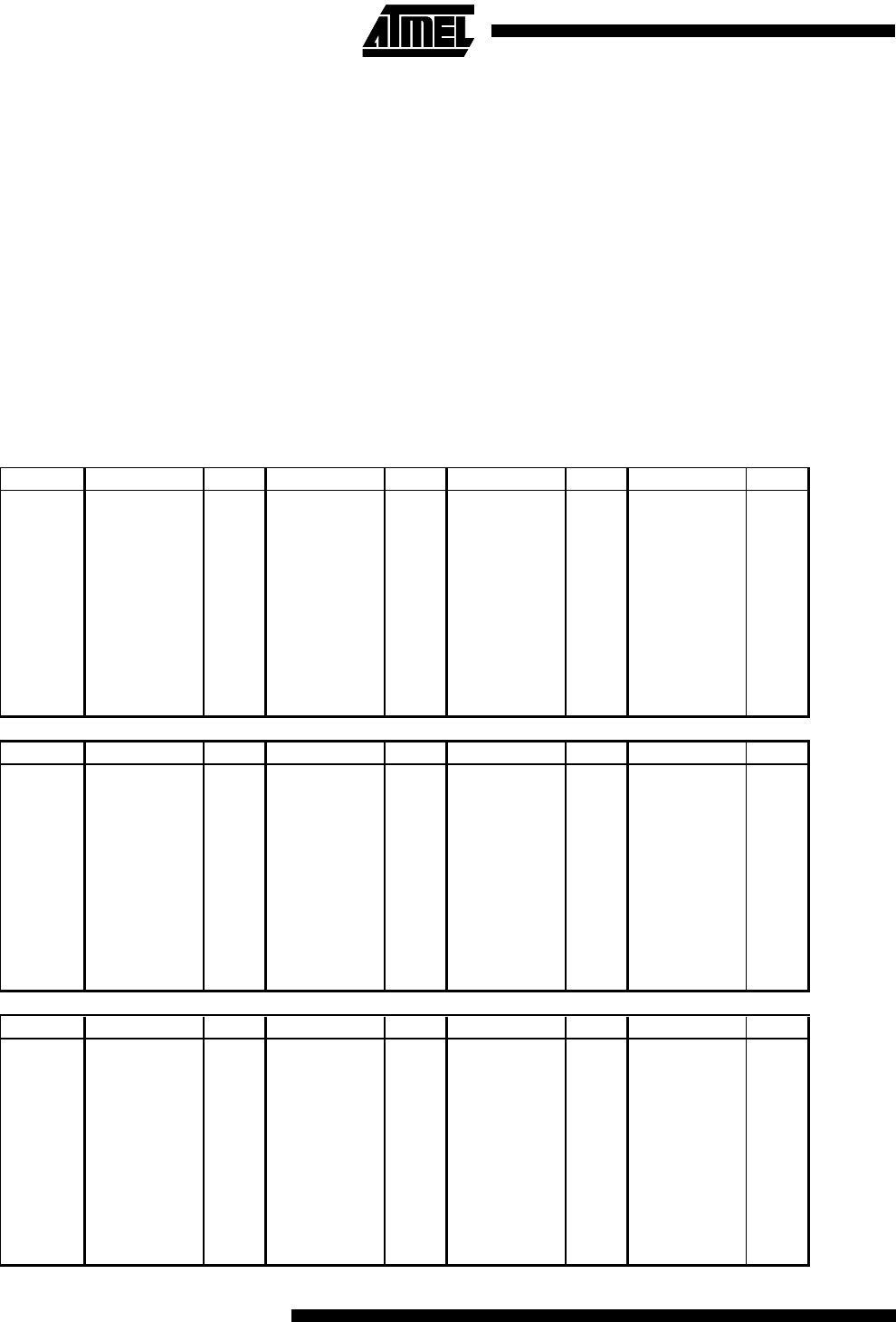
Table 25. UBRR Settings at Various CPU Frequencies
BAUD
f
CK
16 UBRR 1+
()
--------------------------------------=
Baud Rate
1MHz
%Error
1.8432 MHz
%Error
2MHz
%Error
2.4576 MHz
%Error
2400
UBRR=
25 0.2
UBRR=
47 0.0
UBRR=
51 0.2
UBRR=
63 0.0
4800
UBRR=
12 0.2
UBRR=
23 0.0
UBRR=
25 0.2
UBRR=
31 0.0
9600
UBRR= 6 7.5 UBRR=
11 0.0
UBRR=
12 0.2
UBRR=
15 0.0
14400
UBRR= 3 7.8 UBRR=
70.0
UBRR= 8 3.7 UBRR= 10 3.1
19200
UBRR= 2 7.8 UBRR=
50.0
UBRR= 6 7.5 UBRR=
70.0
28800
UBRR= 1 7.8 UBRR=
30.0
UBRR= 3 7.8 UBRR= 4 6.3
38400
UBRR= 1 22.9 UBRR=
20.0
UBRR= 2 7.8 UBRR=
30.0
57600
UBRR= 0 7.8 UBRR=
10.0
UBRR= 1 7.8 UBRR= 2 12.5
76800
UBRR= 0 22.9 UBRR= 1 33.3 UBRR= 1 22.9 UBRR=
10.0
115200
UBRR= 0 84.3 UBRR=
00.0
UBRR= 0 7.8 UBRR= 0 25.0
Baud Rate
3.2768 MHz
%Error
3.6864 MHz
%Error
4MHz
%Error
4.608 MHz
%Error
2400
UBRR=
84 0.4
UBRR=
95 0.0
UBRR=
103 0.2
UBRR=
119 0.0
4800
UBRR=
42 0.8
UBRR=
47 0.0
UBRR=
51 0.2
UBRR=
59 0.0
9600
UBRR=
20 1.6
UBRR=
23 0.0
UBRR=
25 0.2
UBRR=
29 0.0
14400
UBRR=
13 1.6
UBRR=
15 0.0
UBRR= 16 2.1 UBRR=
19 0.0
19200
UBRR= 10 3.1 UBRR=
11 0.0
UBRR=
12 0.2
UBRR=
14 0.0
28800
UBRR=
61.6
UBRR=
70.0
UBRR= 8 3.7 UBRR=
90.0
38400
UBRR= 4 6.3 UBRR=
50.0
UBRR= 6 7.5 UBRR= 7 6.7
57600
UBRR= 3 12.5 UBRR=
30.0
UBRR= 3 7.8 UBRR=
40.0
76800
UBRR= 2 12.5 UBRR=
20.0
UBRR= 2 7.8 UBRR= 3 6.7
115200
UBRR= 1 12.5 UBRR=
10.0
UBRR= 1 7.8 UBRR= 2 20.0
Baud Rate
7.3728 MHz
%Error
8MHz
%Error
9.216 MHz
%Error
11.059 MHz
%Error
2400
UBRR=
191 0.0
UBRR=
207 0.2
UBRR=
239 0.0
UBRR= 287 -
4800
UBRR=
95 0.0
UBRR=
103 0.2
UBRR=
119 0.0
UBRR=
143 0.0
9600
UBRR=
47 0.0
UBRR=
51 0.2
UBRR=
59 0.0
UBRR=
71 0.0
14400
UBRR=
31 0.0
UBRR=
34 0.8
UBRR=
39 0.0
UBRR=
47 0.0
19200
UBRR=
23 0.0
UBRR=
25 0.2
UBRR=
29 0.0
UBRR=
35 0.0
28800
UBRR=
15 0.0
UBRR= 16 2.1 UBRR=
19 0.0
UBRR=
23 0.0
38400
UBRR=
11 0.0
UBRR=
12 0.2
UBRR=
14 0.0
UBRR=
17 0.0
57600
UBRR=
70.0
UBRR= 8 3.7 UBRR=
90.0
UBRR=
11 0.0
76800
UBRR=
50.0
UBRR= 6 7.5 UBRR= 7 6.7 UBRR=
80.0
115200
UBRR=
30.0
UBRR= 3 7.8 UBRR=
40.0
UBRR=
50.0