
Manual


Table Of Contents
- Ordering Information
- Features
- Description
- Architectural Overview
- General Purpose Register File
- ALU - Arithmetic Logic Unit
- ISP Flash Program Memory
- SRAM Data Memory
- Program and Data Addressing Modes
- Register Direct, Single Register Rd
- Register Direct, Two Registers Rd and Rr
- I/O Direct
- Data Direct
- Data Indirect with Displacement
- Data Indirect
- Data Indirect With Pre-Decrement
- Data Indirect With Post-Increment
- Constant Addressing Using the LPM and ELPM Instructions
- Direct Program Address, JMP and CALL
- Indirect Program Addressing, IJMP and ICALL
- Relative Program Addressing, RJMP and RCALL
- EEPROM Data Memory
- Memory Access Times and Instruction Execution Timing
- I/O Memory
- Reset and Interrupt Handling
- Reset Sources
- Power-On Reset
- External Reset
- Watchdog Reset
- MCU Status Register - MCUSR
- Interrupt Handling
- External Interrupt Mask Register - EIMSK
- External Interrupt Flag Register - EIFR
- External Interrupt Control Register - EICR
- Timer/Counter Interrupt Mask Register - TIMSK
- Timer/Counter Interrupt Flag Register - TIFR
- Interrupt Response Time
- Sleep Modes
- Timer/Counters
- Timer/Counter Prescalers
- 8-bit Timer/Counters T/C0 and T/C2
- Timer/Counter0 Control Register - TCCR0
- Timer/Counter2 Control Register - TCCR2
- Timer/Counter0 - TCNT0
- Timer/Counter2 - TCNT2
- Timer/Counter0 Output Compare Register - OCR0
- Timer/Counter2 Output Compare Register - OCR2
- Timer/Counter 0 and 2 in PWM mode
- Asynchronous Status Register - ASSR
- Asynchronous Operation of Timer/Counter0
- 16-bit Timer/Counter1
- Timer/Counter1 Control Register A - TCCR1A
- Timer/Counter1 Control Register B - TCCR1B
- Timer/Counter1 - TCNT1H and TCNT1L
- Timer/Counter1 Output Compare Register - OCR1AH and OCR1AL
- Timer/Counter1 Output Compare Register - OCR1BH and OCR1BL
- Timer/Counter1 Input Capture Register - ICR1H and ICR1L
- Timer/Counter1 in PWM mode
- Watchdog Timer
- EEPROM Read/Write Access
- Serial Peripheral Interface - SPI
- UART
- Analog Comparator
- Analog to Digital Converter
- Interface to external SRAM
- I/O-Ports
- Memory Programming
- Electrical Characteristics
- Typical characteristics
- Register Summary
- Instruction Set Summary (Continued)
ATmega603/103
61
Data Reception
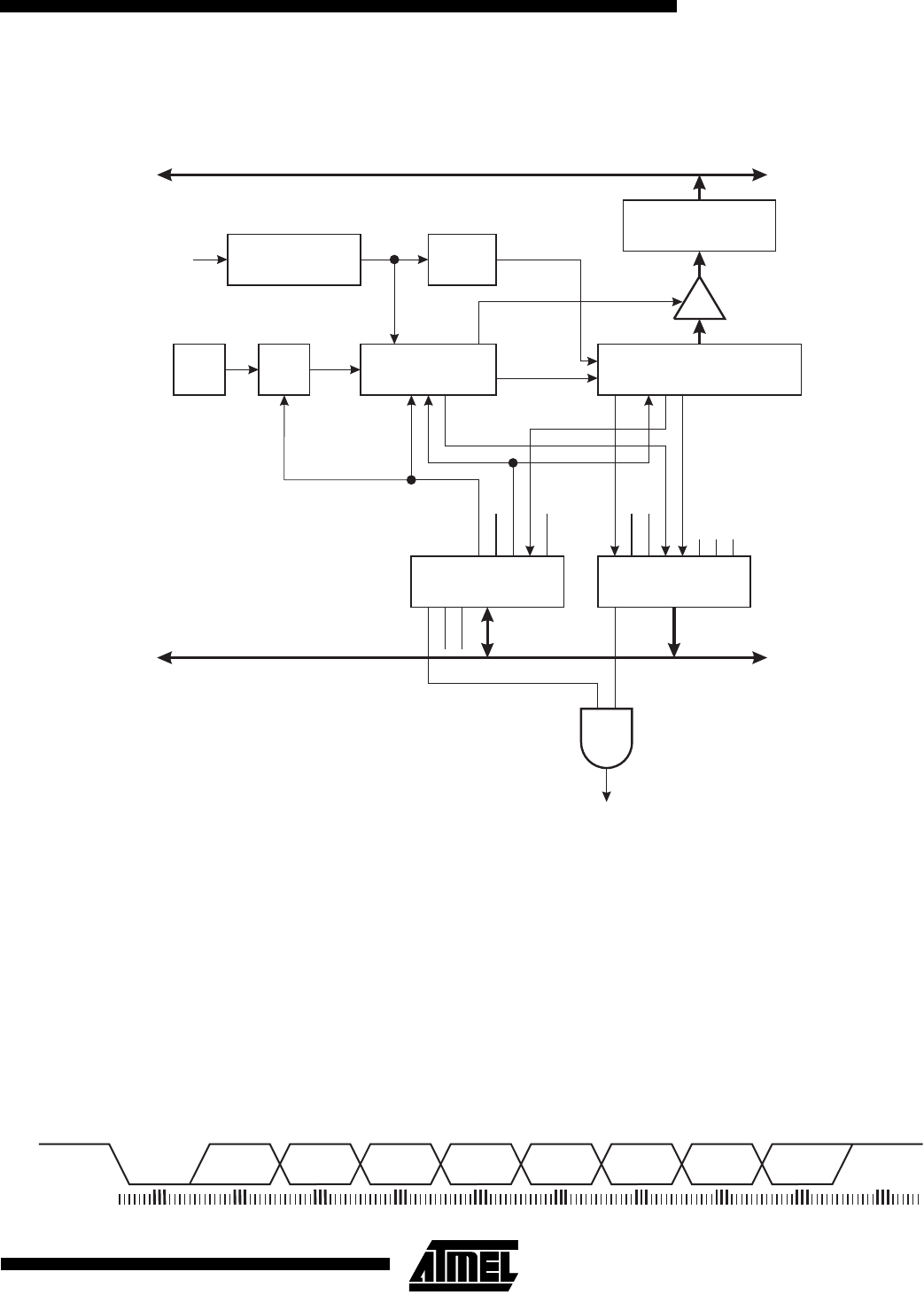
Figure 42. UART Receiver
The receiver front-end logic samples the signal on the RXD pin at a frequency 16 times the baud rate. While the line is idle,
one single sample of logical zero will be interpreted as the falling edge of a start bit, and the start bit detection sequence is
initiated. Let sample 1 denote the first zero-sample. Following the 1 to 0-transition, the receiver samples the RXD pin at
sample 8, 9, and 10. If two or more of these three samples are found to be logical ones, the start bit is rejected as a noise
spike and the receiver starts looking for the next 1 to 0-transition.
If however, a valid start bit is detected, sampling of the data bits following the start bit is performed. These bits are also
sampled at samples 8, 9, and 10. The logical value found in at least two of the three samples is taken as the bit value. All
bits are shifted into the transmitter shift register as they are sampled. Sampling of an incoming character is shown in Figure
43.
Figure 43. Sampling Received Data
DATA BUS
DATA BUS
UART I/O DATA
REGISTER (UDR)
10(11)-BIT RX
SHIFT REGISTER
UART CONTROL
REGISTER (UCR)
DATA RECOVERY
LOGIC
UART STATUS
REGISTER (USR)
BAUD RATE
GENERATOR
XTAL
RXB8
TXB8
TXEN
CHR9
RXEN
TXC
TXCIE
RXCIE
UDRIE
UDRE
RXC
RXC
FE
DOR
RXC
IRQ
/16
BAUD X 16 BAUD
STORE UDR
PIN CONTROL
LOGIC
RXD
START BIT D0 D1 D2 D3 D4 D5 D6 D7 STOP BIT
RXD
RECEIVER
SAMPLING