
Manual


Table Of Contents
- Ordering Information
- Features
- Description
- Architectural Overview
- General Purpose Register File
- ALU - Arithmetic Logic Unit
- ISP Flash Program Memory
- SRAM Data Memory
- Program and Data Addressing Modes
- Register Direct, Single Register Rd
- Register Direct, Two Registers Rd and Rr
- I/O Direct
- Data Direct
- Data Indirect with Displacement
- Data Indirect
- Data Indirect With Pre-Decrement
- Data Indirect With Post-Increment
- Constant Addressing Using the LPM and ELPM Instructions
- Direct Program Address, JMP and CALL
- Indirect Program Addressing, IJMP and ICALL
- Relative Program Addressing, RJMP and RCALL
- EEPROM Data Memory
- Memory Access Times and Instruction Execution Timing
- I/O Memory
- Reset and Interrupt Handling
- Reset Sources
- Power-On Reset
- External Reset
- Watchdog Reset
- MCU Status Register - MCUSR
- Interrupt Handling
- External Interrupt Mask Register - EIMSK
- External Interrupt Flag Register - EIFR
- External Interrupt Control Register - EICR
- Timer/Counter Interrupt Mask Register - TIMSK
- Timer/Counter Interrupt Flag Register - TIFR
- Interrupt Response Time
- Sleep Modes
- Timer/Counters
- Timer/Counter Prescalers
- 8-bit Timer/Counters T/C0 and T/C2
- Timer/Counter0 Control Register - TCCR0
- Timer/Counter2 Control Register - TCCR2
- Timer/Counter0 - TCNT0
- Timer/Counter2 - TCNT2
- Timer/Counter0 Output Compare Register - OCR0
- Timer/Counter2 Output Compare Register - OCR2
- Timer/Counter 0 and 2 in PWM mode
- Asynchronous Status Register - ASSR
- Asynchronous Operation of Timer/Counter0
- 16-bit Timer/Counter1
- Timer/Counter1 Control Register A - TCCR1A
- Timer/Counter1 Control Register B - TCCR1B
- Timer/Counter1 - TCNT1H and TCNT1L
- Timer/Counter1 Output Compare Register - OCR1AH and OCR1AL
- Timer/Counter1 Output Compare Register - OCR1BH and OCR1BL
- Timer/Counter1 Input Capture Register - ICR1H and ICR1L
- Timer/Counter1 in PWM mode
- Watchdog Timer
- EEPROM Read/Write Access
- Serial Peripheral Interface - SPI
- UART
- Analog Comparator
- Analog to Digital Converter
- Interface to external SRAM
- I/O-Ports
- Memory Programming
- Electrical Characteristics
- Typical characteristics
- Register Summary
- Instruction Set Summary (Continued)
ATmega603/103
60
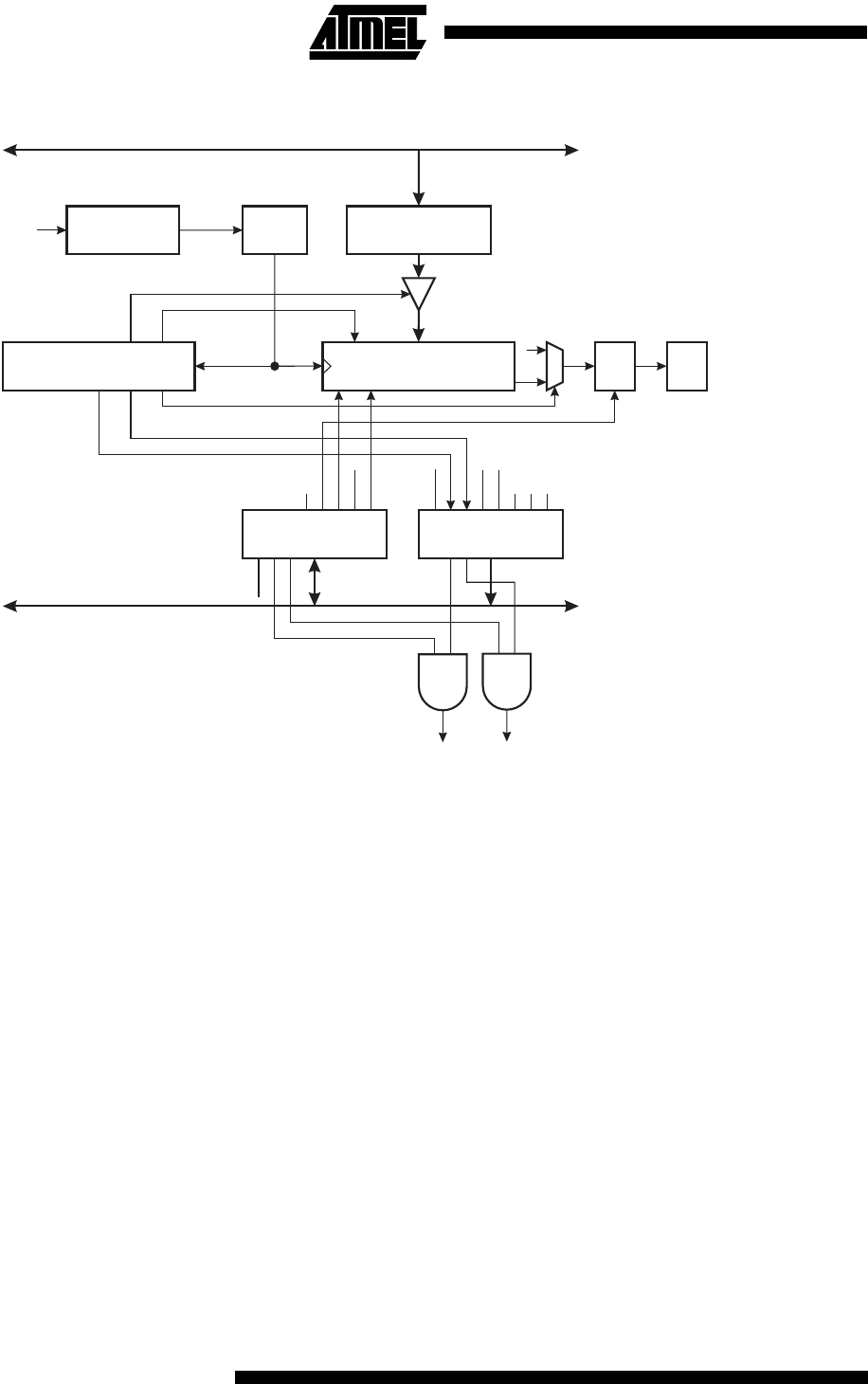
Figure 41. UART Transmitter
On the Baud Rate clock following the transfer operation to the shift register, the start bit is shifted out on the TXD pin, fol-
lowed by the data, LSB first. When the stop bit has been shifted out, the shift register is loaded if any new data has been
written to the UDR during the transmission. During loading, UDRE is set. If there is no new data in the UDR register to send
when the stop bit is shifted out, the UDRE flag will remain set. In this case, after the stop bit has been present on TXD for
one bit length, the TX Complete Flag, TXC, in USR is set.
The TXEN bit in UCR enables the UART transmitter when set (one). When this bit is cleared (zero), the PE1 pin can be
used for general I/O. When TXEN is set, the UART Transmitter will be connected to PE1, which is forced to be an output
pin regardless of the setting of the DDE1 bit in DDRE.
DATA BUS
DATA BUS
UART I/O DATA
REGISTER (UDR)
10(11)-BIT TX
SHIFT REGISTER
UART CONTROL
REGISTER (UCR)
CONTROL LOGIC
UART STATUS
REGISTER (USR)
BAUD RATE
GENERATOR
XTAL
TXB8
RXB8
TXEN
CHR9
RXEN
TXCTXC
TXCIE
RXCIE
UDRIE
UDRE
RXC
FE
OR
UDRE
/16
UDRE
IRQ
TXC
IRQ
SHIFT ENABLE
STORE UDR
1
IDLE
BAUD
BAUD x 16
PIN CONTROL
LOGIC
TXD