
Manual


Table Of Contents
- Ordering Information
- Features
- Description
- Architectural Overview
- General Purpose Register File
- ALU - Arithmetic Logic Unit
- ISP Flash Program Memory
- SRAM Data Memory
- Program and Data Addressing Modes
- Register Direct, Single Register Rd
- Register Direct, Two Registers Rd and Rr
- I/O Direct
- Data Direct
- Data Indirect with Displacement
- Data Indirect
- Data Indirect With Pre-Decrement
- Data Indirect With Post-Increment
- Constant Addressing Using the LPM and ELPM Instructions
- Direct Program Address, JMP and CALL
- Indirect Program Addressing, IJMP and ICALL
- Relative Program Addressing, RJMP and RCALL
- EEPROM Data Memory
- Memory Access Times and Instruction Execution Timing
- I/O Memory
- Reset and Interrupt Handling
- Reset Sources
- Power-On Reset
- External Reset
- Watchdog Reset
- MCU Status Register - MCUSR
- Interrupt Handling
- External Interrupt Mask Register - EIMSK
- External Interrupt Flag Register - EIFR
- External Interrupt Control Register - EICR
- Timer/Counter Interrupt Mask Register - TIMSK
- Timer/Counter Interrupt Flag Register - TIFR
- Interrupt Response Time
- Sleep Modes
- Timer/Counters
- Timer/Counter Prescalers
- 8-bit Timer/Counters T/C0 and T/C2
- Timer/Counter0 Control Register - TCCR0
- Timer/Counter2 Control Register - TCCR2
- Timer/Counter0 - TCNT0
- Timer/Counter2 - TCNT2
- Timer/Counter0 Output Compare Register - OCR0
- Timer/Counter2 Output Compare Register - OCR2
- Timer/Counter 0 and 2 in PWM mode
- Asynchronous Status Register - ASSR
- Asynchronous Operation of Timer/Counter0
- 16-bit Timer/Counter1
- Timer/Counter1 Control Register A - TCCR1A
- Timer/Counter1 Control Register B - TCCR1B
- Timer/Counter1 - TCNT1H and TCNT1L
- Timer/Counter1 Output Compare Register - OCR1AH and OCR1AL
- Timer/Counter1 Output Compare Register - OCR1BH and OCR1BL
- Timer/Counter1 Input Capture Register - ICR1H and ICR1L
- Timer/Counter1 in PWM mode
- Watchdog Timer
- EEPROM Read/Write Access
- Serial Peripheral Interface - SPI
- UART
- Analog Comparator
- Analog to Digital Converter
- Interface to external SRAM
- I/O-Ports
- Memory Programming
- Electrical Characteristics
- Typical characteristics
- Register Summary
- Instruction Set Summary (Continued)
ATmega603/103
6
Clock Options
Crystal Oscillator
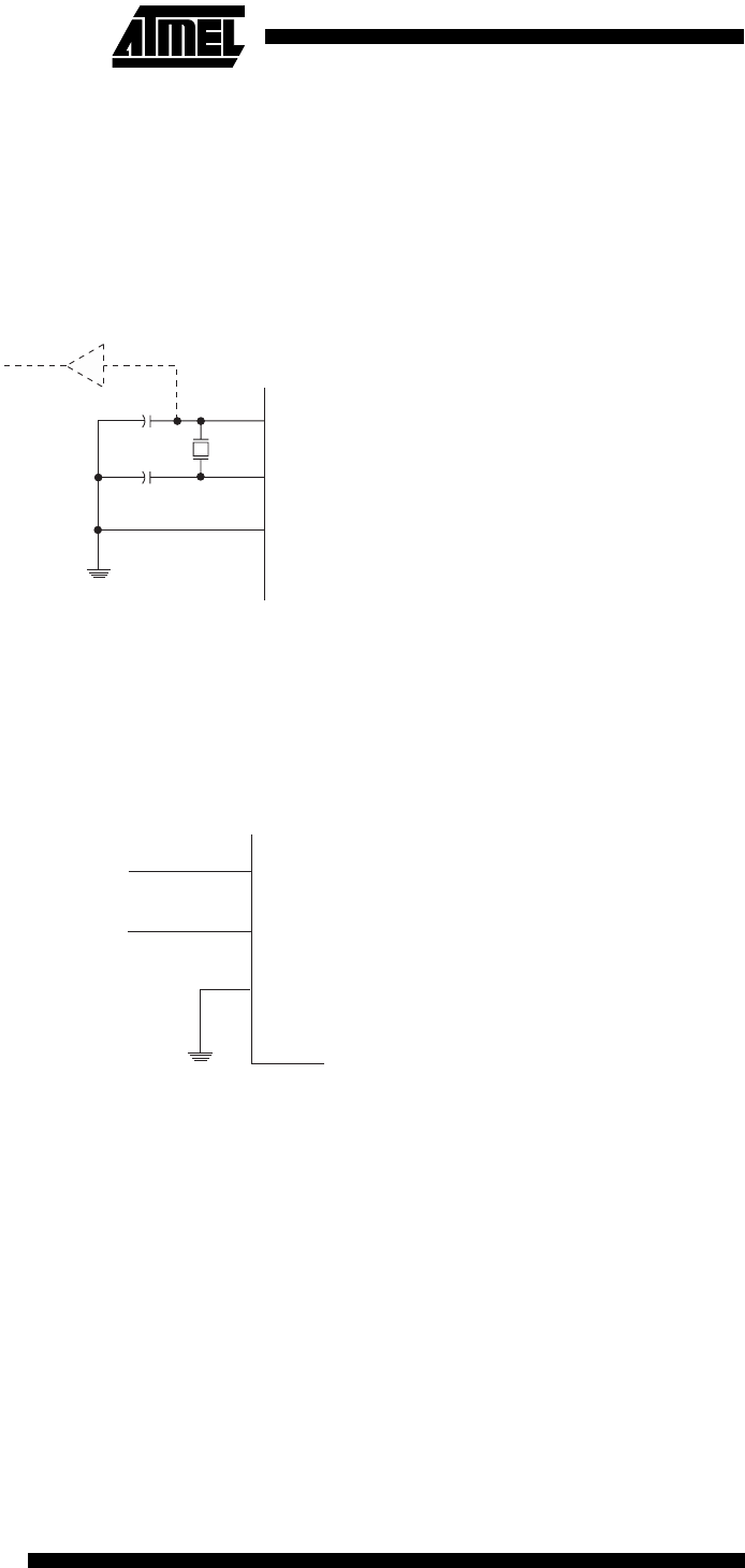
XTAL1 and XTAL2 are input and output, respectively, of an inverting amplifier which can be configured for use as an on-
chip oscillator, as shown in Figure 2. Either a quartz crystal or a ceramic resonator may be used.
Figure 2. Oscillator Connections
Note: When using the MCU Oscillator as a clock for an external device, an HC buffer should be connected as indicated in the figure.
External Clock
To drive the device from an external clock source, XTAL2 should be left unconnected while XTAL1 is driven as shown in
Figure 3.
Figure 3. External Clock Drive Configuration
Timer Oscillator
For the Timer Oscillator pins, TOSC1 and TOSC2, the crystal is connected directly between the pins. No external capaci-
tors are needed. The oscillator is optimized for use with a 32,768 Hz watch crystal. An external clock signal applied to this
pin goes through the same amplifier having a bandwidth of 256 kHz. The external clock signal should therefore be in the
range 0 Hz - 256 kHz.
XTAL2
XTAL1
GND
C2
C1
MAX 1 HC BUFFER
HC
XTAL2
XTAL1
GND
NC
EXTERNAL
OSCILLATOR
SIGNAL