
Manual


Table Of Contents
- Ordering Information
- Features
- Description
- Architectural Overview
- General Purpose Register File
- ALU - Arithmetic Logic Unit
- ISP Flash Program Memory
- SRAM Data Memory
- Program and Data Addressing Modes
- Register Direct, Single Register Rd
- Register Direct, Two Registers Rd and Rr
- I/O Direct
- Data Direct
- Data Indirect with Displacement
- Data Indirect
- Data Indirect With Pre-Decrement
- Data Indirect With Post-Increment
- Constant Addressing Using the LPM and ELPM Instructions
- Direct Program Address, JMP and CALL
- Indirect Program Addressing, IJMP and ICALL
- Relative Program Addressing, RJMP and RCALL
- EEPROM Data Memory
- Memory Access Times and Instruction Execution Timing
- I/O Memory
- Reset and Interrupt Handling
- Reset Sources
- Power-On Reset
- External Reset
- Watchdog Reset
- MCU Status Register - MCUSR
- Interrupt Handling
- External Interrupt Mask Register - EIMSK
- External Interrupt Flag Register - EIFR
- External Interrupt Control Register - EICR
- Timer/Counter Interrupt Mask Register - TIMSK
- Timer/Counter Interrupt Flag Register - TIFR
- Interrupt Response Time
- Sleep Modes
- Timer/Counters
- Timer/Counter Prescalers
- 8-bit Timer/Counters T/C0 and T/C2
- Timer/Counter0 Control Register - TCCR0
- Timer/Counter2 Control Register - TCCR2
- Timer/Counter0 - TCNT0
- Timer/Counter2 - TCNT2
- Timer/Counter0 Output Compare Register - OCR0
- Timer/Counter2 Output Compare Register - OCR2
- Timer/Counter 0 and 2 in PWM mode
- Asynchronous Status Register - ASSR
- Asynchronous Operation of Timer/Counter0
- 16-bit Timer/Counter1
- Timer/Counter1 Control Register A - TCCR1A
- Timer/Counter1 Control Register B - TCCR1B
- Timer/Counter1 - TCNT1H and TCNT1L
- Timer/Counter1 Output Compare Register - OCR1AH and OCR1AL
- Timer/Counter1 Output Compare Register - OCR1BH and OCR1BL
- Timer/Counter1 Input Capture Register - ICR1H and ICR1L
- Timer/Counter1 in PWM mode
- Watchdog Timer
- EEPROM Read/Write Access
- Serial Peripheral Interface - SPI
- UART
- Analog Comparator
- Analog to Digital Converter
- Interface to external SRAM
- I/O-Ports
- Memory Programming
- Electrical Characteristics
- Typical characteristics
- Register Summary
- Instruction Set Summary (Continued)
ATmega603/103
57
Data Modes
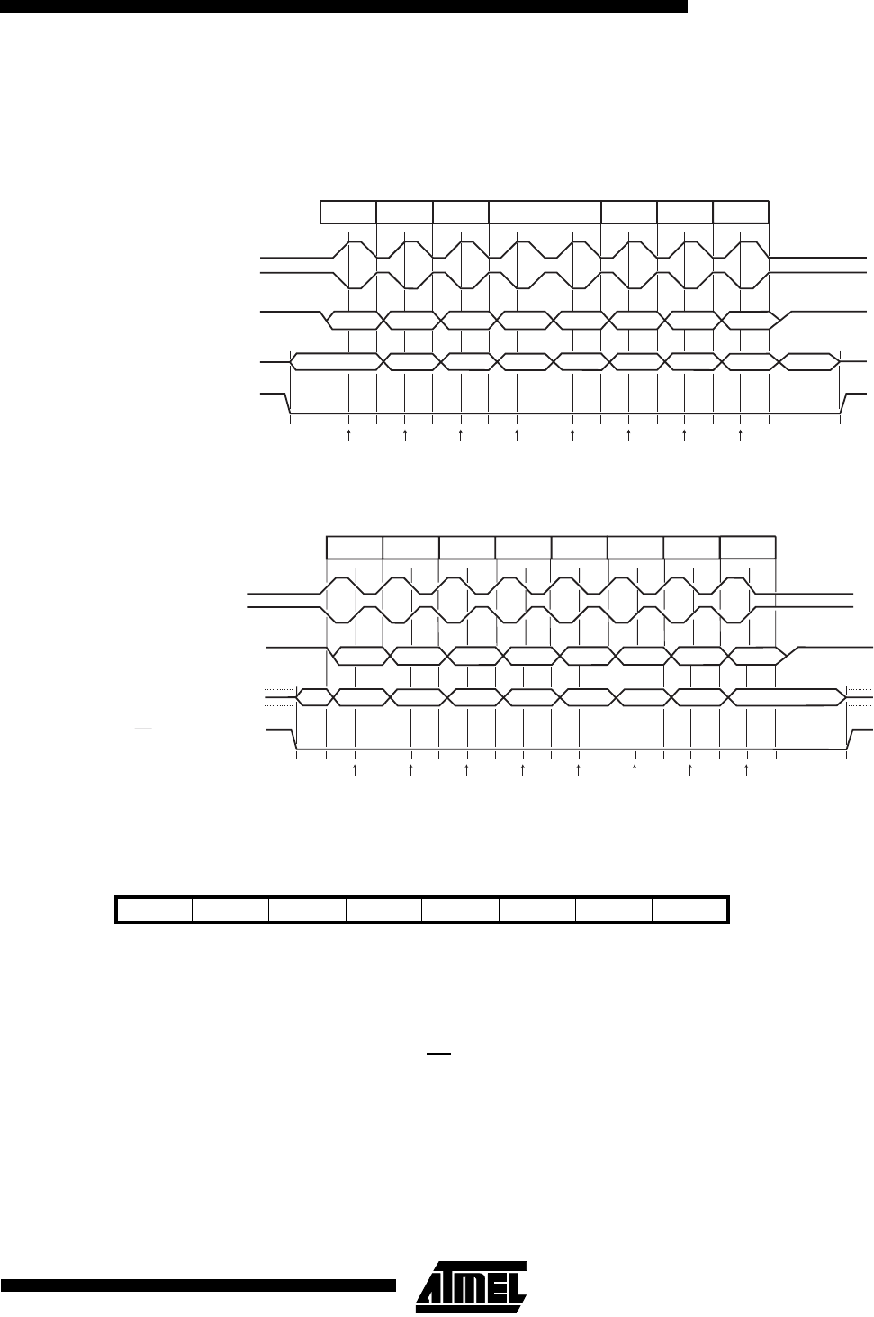
There are four combinations of SCK phase and polarity with respect to serial data, which are determined by control bits
CPHA and CPOL. The SPI data transfer formats are shown in Figure 39 and Figure 40.
Figure 39. SPI Transfer Format with CPHA = 0 and DORD = 0
Figure 40. SPI Transfer Format with CPHA = 1and DORD = 0
SPI Control Register - SPCR
•
Bit 7 - SPIE: SPI Interrupt Enable
This bit causes the SPI interrupt to be executed if SPIF bit in the SPSR register is set and the global interrupts are enabled.
•
Bit 6 - SPE: SPI Enable
When the SPE bit is set (one), the SPI is enabled and SS, MOSI, MISO and SCK are connected to pins PB0, PB1, PB2 and
PB3.
•
Bit 5 - DORD: Data Order
When the DORD bit is set (one), the LSB of the data word is transmitted first.
When the DORD bit is cleared (zero), the MSB of the data word is transmitted first.
Bit 76543210
$0D ($2D) SPIE SPE DORD MSTR CPOL CPHA SPR1 SPR0 SPCR
Read/Write R/W R/W R/W R/W R/W R/W R/W R/W
Initial value00000000
MSB 6 5 4 3 2 1 LSB
1 2 3 4 5 6 7 8
MSB
6 5 4 3 2 1 LSB
*
SCK CYCLE #
(FOR REFERENCE)
SCK (CPOL=0)
SCK (CPOL=1)
MOSI
(FROM MASTER)
MISO
(FROM SLAVE)
SS (TO SLAVE)
* Not defined but normally MSB of character just received
SAMPLE
1
1
1
2
2
2
3
3
3
4
4
4
5
5
5
6
6
6
*
78
SCK CYCLE #
(FOR REFERENCE)
SCK (CPOL=0)
SCK (CPOL=1)
MOSI
(FROM MASTER)
MISO
(FROM SLAVE)
SS (TO SLAVE)
* Not defined but normally LSB of previously transmitted character.
MSB LSB
LSBMSB
SAMPLE