
Manual


Table Of Contents
- Ordering Information
- Features
- Description
- Architectural Overview
- General Purpose Register File
- ALU - Arithmetic Logic Unit
- ISP Flash Program Memory
- SRAM Data Memory
- Program and Data Addressing Modes
- Register Direct, Single Register Rd
- Register Direct, Two Registers Rd and Rr
- I/O Direct
- Data Direct
- Data Indirect with Displacement
- Data Indirect
- Data Indirect With Pre-Decrement
- Data Indirect With Post-Increment
- Constant Addressing Using the LPM and ELPM Instructions
- Direct Program Address, JMP and CALL
- Indirect Program Addressing, IJMP and ICALL
- Relative Program Addressing, RJMP and RCALL
- EEPROM Data Memory
- Memory Access Times and Instruction Execution Timing
- I/O Memory
- Reset and Interrupt Handling
- Reset Sources
- Power-On Reset
- External Reset
- Watchdog Reset
- MCU Status Register - MCUSR
- Interrupt Handling
- External Interrupt Mask Register - EIMSK
- External Interrupt Flag Register - EIFR
- External Interrupt Control Register - EICR
- Timer/Counter Interrupt Mask Register - TIMSK
- Timer/Counter Interrupt Flag Register - TIFR
- Interrupt Response Time
- Sleep Modes
- Timer/Counters
- Timer/Counter Prescalers
- 8-bit Timer/Counters T/C0 and T/C2
- Timer/Counter0 Control Register - TCCR0
- Timer/Counter2 Control Register - TCCR2
- Timer/Counter0 - TCNT0
- Timer/Counter2 - TCNT2
- Timer/Counter0 Output Compare Register - OCR0
- Timer/Counter2 Output Compare Register - OCR2
- Timer/Counter 0 and 2 in PWM mode
- Asynchronous Status Register - ASSR
- Asynchronous Operation of Timer/Counter0
- 16-bit Timer/Counter1
- Timer/Counter1 Control Register A - TCCR1A
- Timer/Counter1 Control Register B - TCCR1B
- Timer/Counter1 - TCNT1H and TCNT1L
- Timer/Counter1 Output Compare Register - OCR1AH and OCR1AL
- Timer/Counter1 Output Compare Register - OCR1BH and OCR1BL
- Timer/Counter1 Input Capture Register - ICR1H and ICR1L
- Timer/Counter1 in PWM mode
- Watchdog Timer
- EEPROM Read/Write Access
- Serial Peripheral Interface - SPI
- UART
- Analog Comparator
- Analog to Digital Converter
- Interface to external SRAM
- I/O-Ports
- Memory Programming
- Electrical Characteristics
- Typical characteristics
- Register Summary
- Instruction Set Summary (Continued)
ATmega603/103
52
Note: The frequency of the watchdog oscillator is voltage dependent as shown in the Electrical Characteristics section.
The WDR - Watchdog Reset - instruction should always be executed before the Watchdog Timer is enabled. This ensures that
the reset period will be in accordance with the Watchdog Timer prescale settings. If the Watchdog Timer is enabled without
reset, the watchdog timer may not start counting from zero.
EEPROM Read/Write Access
The EEPROM access registers are accessible in the I/O space.
The write access time is in the range of 2.5 - 4ms, depending on the V
CC
voltages. A self-timing function lets the user soft-
ware detect when the next byte can be written. A special EEPROM Ready interrupt can be set to trigger when the
EEPROM is ready to accept new data.
In order to prevent unintentional EEPROM writes, a specific write procedure must be followed. Refer to the description of
the EEPROM control register for details on this.
When the EEPROM is written, the CPU is halted for two clock cycles before the next instruction is executed. When it is
read, the CPU is halted for 4 clock cycles.
EEPROM Address Register - EEARH, EEARL
The EEPROM Address Registers - EEARH and EEARL specify the EEPROM address in the 2K/4K-byte EEPROM space.
The EEPROM data bytes are addressed linearly between 0 and 2047/4095. The ATmega603 has an EEPROM address
space of 2K, and the EEAR11 I/O bit is read-only with initial value of 0.
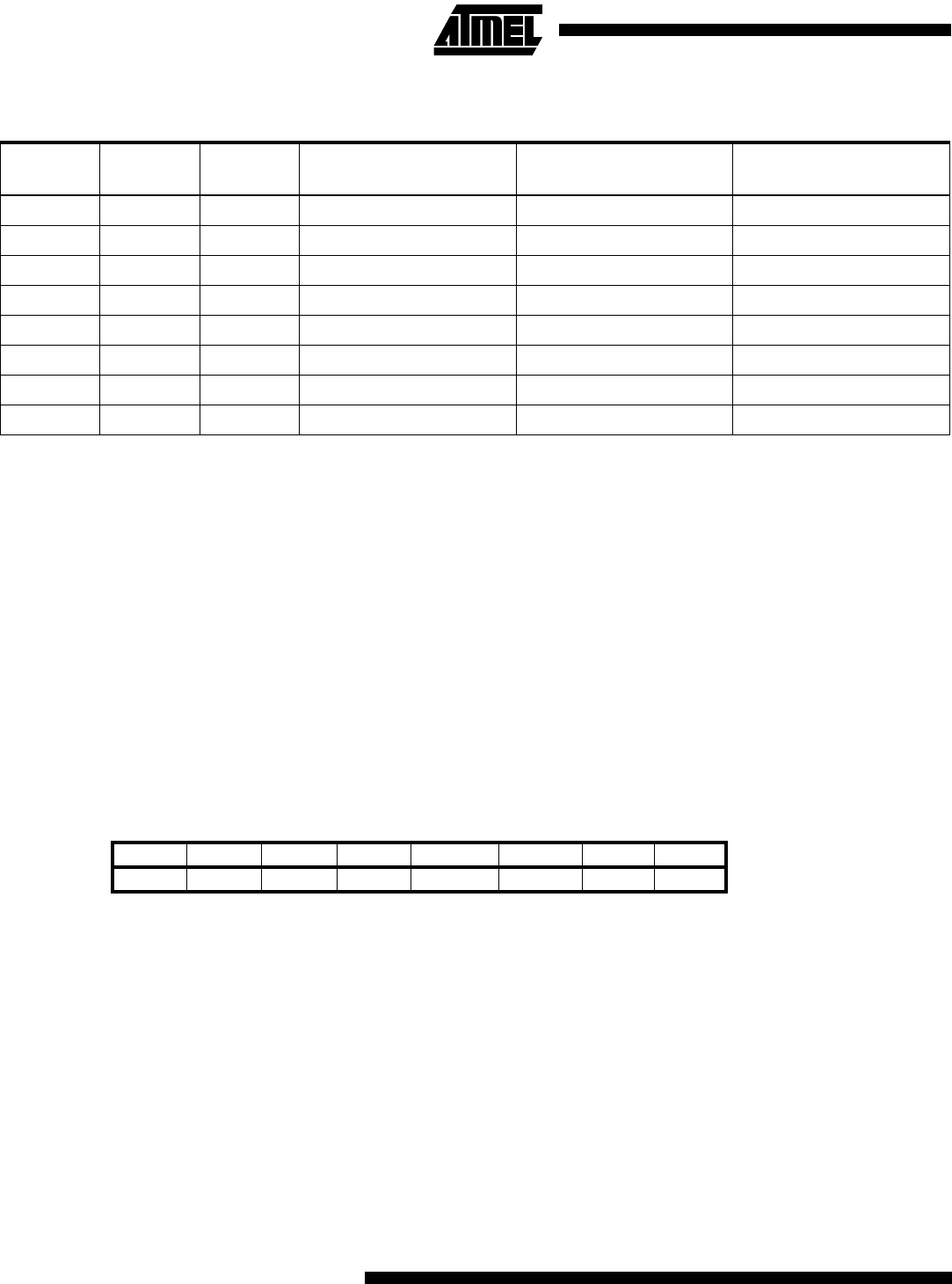
Table 22. Watch Dog Timer Prescale Select
WDP2 WDP1 WDP0
Number of WDT Oscillator
cycles
Typical time-out
at Vcc = 3.0V
Typical time-out
at Vcc = 5.0V
0 0 0 16K cycles 47 ms 15 ms
0 0 1 32K cycles 94 ms 30 ms
0 1 0 64K cycles 0.19 s 60 ms
0 1 1 128K cycles 0.38 s 0.12 s
1 0 0 256K cycles 0.75 s 0,24 s
1 0 1 512K cycles 1.5 s 0.49 s
1 1 0 1,024K cycles 3.0 s 0.97 s
1 1 1 2,048K cycles 6.0 s 1.9 s
Bit 15141312 11 10 9 8
$1F ($3F) - - - - EEAR11 EEAR10 EEAR9 EEAR8 EEARH
$1E ($3E) EEAR7 EEAR6 EEAR5 EEAR4 EEAR3 EEAR2 EEAR1 EEAR0 EEARL
7654 3 2 10
Read/Write R R R R R/W R/W R/W R/W
R/W R/W R/W R/W R/W R/W R/W R/W
Initial value 0 0 0 0 0 0 0 0
0000 0 0 00