
Manual


Table Of Contents
- Ordering Information
- Features
- Description
- Architectural Overview
- General Purpose Register File
- ALU - Arithmetic Logic Unit
- ISP Flash Program Memory
- SRAM Data Memory
- Program and Data Addressing Modes
- Register Direct, Single Register Rd
- Register Direct, Two Registers Rd and Rr
- I/O Direct
- Data Direct
- Data Indirect with Displacement
- Data Indirect
- Data Indirect With Pre-Decrement
- Data Indirect With Post-Increment
- Constant Addressing Using the LPM and ELPM Instructions
- Direct Program Address, JMP and CALL
- Indirect Program Addressing, IJMP and ICALL
- Relative Program Addressing, RJMP and RCALL
- EEPROM Data Memory
- Memory Access Times and Instruction Execution Timing
- I/O Memory
- Reset and Interrupt Handling
- Reset Sources
- Power-On Reset
- External Reset
- Watchdog Reset
- MCU Status Register - MCUSR
- Interrupt Handling
- External Interrupt Mask Register - EIMSK
- External Interrupt Flag Register - EIFR
- External Interrupt Control Register - EICR
- Timer/Counter Interrupt Mask Register - TIMSK
- Timer/Counter Interrupt Flag Register - TIFR
- Interrupt Response Time
- Sleep Modes
- Timer/Counters
- Timer/Counter Prescalers
- 8-bit Timer/Counters T/C0 and T/C2
- Timer/Counter0 Control Register - TCCR0
- Timer/Counter2 Control Register - TCCR2
- Timer/Counter0 - TCNT0
- Timer/Counter2 - TCNT2
- Timer/Counter0 Output Compare Register - OCR0
- Timer/Counter2 Output Compare Register - OCR2
- Timer/Counter 0 and 2 in PWM mode
- Asynchronous Status Register - ASSR
- Asynchronous Operation of Timer/Counter0
- 16-bit Timer/Counter1
- Timer/Counter1 Control Register A - TCCR1A
- Timer/Counter1 Control Register B - TCCR1B
- Timer/Counter1 - TCNT1H and TCNT1L
- Timer/Counter1 Output Compare Register - OCR1AH and OCR1AL
- Timer/Counter1 Output Compare Register - OCR1BH and OCR1BL
- Timer/Counter1 Input Capture Register - ICR1H and ICR1L
- Timer/Counter1 in PWM mode
- Watchdog Timer
- EEPROM Read/Write Access
- Serial Peripheral Interface - SPI
- UART
- Analog Comparator
- Analog to Digital Converter
- Interface to external SRAM
- I/O-Ports
- Memory Programming
- Electrical Characteristics
- Typical characteristics
- Register Summary
- Instruction Set Summary (Continued)
ATmega603/103
51
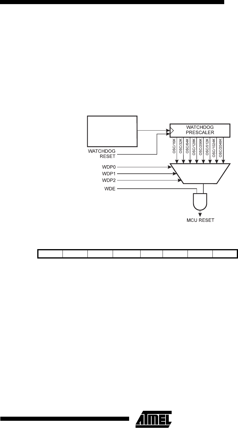
Watchdog Timer
The Watchdog Timer is clocked from a separate on-chip oscillator. By controlling the Watchdog Timer prescaler, the
Watchdog reset interval can be adjusted as shown in Table 22. See characterization data for typical values at other V
CC
levels. The WDR - Watchdog Reset - instruction resets the Watchdog Timer. From the Watchdog is reset, eight different
clock cycle periods can be selected to determine the reset period. If the reset period expires without another Watchdog
reset, the ATmega603/103 resets and executes from the reset vector. For timing details on the Watchdog reset, refer to
page 28.
To prevent unintentional disabling of the watchdog, a special turn-off procedure must be followed when the watchdog is
disabled. Refer to the description of the Watchdog Timer Control Register for details.
Figure 36. Watchdog Timer
Watchdog Timer Control Register - WDTCR
•
Bits 7..5 - Res: Reserved bits
These bits are reserved bits in the ATmega603/103 and will always read as zero.
•
Bit 4 - WDTOE: Watch Dog Turn Off Enable
This bit must be set (one) when the WDE bit is cleared, Otherwise, the watchdog will not be disabled. Once set, hardware
will clear this bit to zero after four clock cycles. Refer to the description of the WDE bit for a watchdog disable procedure.
•
Bit 3 - WDE: Watch Dog Enable
When the WDE is set (one) the Watchdog Timer is enabled, and if the WDE is cleared (zero) the Watchdog Timer function
is disabled. WDE can only be cleared if the WDTOE bit is set (one). To disable an enabled watchdog timer, the following
procedure must be followed:
1. In the same operation, write a logical one to WDTOE and WDE. A logical one must be written to WDE even though
it is set to one before the disable operation starts.
2. Within the next four clock cycles, write a logical 0 to WDE. This disables the watchdog.
•
Bits 2..0 - WDP2, WDP1, WDP0: Watch Dog Timer Prescaler 2, 1 and 0
The WDP2, WDP1 and WDP0 bits determine the Watchdog Timer prescaling when the Watchdog Timer is enabled. The
different prescaling values and their corresponding Time-out Periods are shown in Table 22.
Bit 765 43210
$21 ($41) - - - WDTOE WDE WDP2 WDP1 WDP0 WDTCR
Read/Write R R R R/W R/W R/W R/W R/W
Initial value 0 0 0 0 0 0 0 0
1 MHz at V
CC
= 5V
350 kHz at V
CC
= 3V
Oscillator