
Manual


Table Of Contents
- Ordering Information
- Features
- Description
- Architectural Overview
- General Purpose Register File
- ALU - Arithmetic Logic Unit
- ISP Flash Program Memory
- SRAM Data Memory
- Program and Data Addressing Modes
- Register Direct, Single Register Rd
- Register Direct, Two Registers Rd and Rr
- I/O Direct
- Data Direct
- Data Indirect with Displacement
- Data Indirect
- Data Indirect With Pre-Decrement
- Data Indirect With Post-Increment
- Constant Addressing Using the LPM and ELPM Instructions
- Direct Program Address, JMP and CALL
- Indirect Program Addressing, IJMP and ICALL
- Relative Program Addressing, RJMP and RCALL
- EEPROM Data Memory
- Memory Access Times and Instruction Execution Timing
- I/O Memory
- Reset and Interrupt Handling
- Reset Sources
- Power-On Reset
- External Reset
- Watchdog Reset
- MCU Status Register - MCUSR
- Interrupt Handling
- External Interrupt Mask Register - EIMSK
- External Interrupt Flag Register - EIFR
- External Interrupt Control Register - EICR
- Timer/Counter Interrupt Mask Register - TIMSK
- Timer/Counter Interrupt Flag Register - TIFR
- Interrupt Response Time
- Sleep Modes
- Timer/Counters
- Timer/Counter Prescalers
- 8-bit Timer/Counters T/C0 and T/C2
- Timer/Counter0 Control Register - TCCR0
- Timer/Counter2 Control Register - TCCR2
- Timer/Counter0 - TCNT0
- Timer/Counter2 - TCNT2
- Timer/Counter0 Output Compare Register - OCR0
- Timer/Counter2 Output Compare Register - OCR2
- Timer/Counter 0 and 2 in PWM mode
- Asynchronous Status Register - ASSR
- Asynchronous Operation of Timer/Counter0
- 16-bit Timer/Counter1
- Timer/Counter1 Control Register A - TCCR1A
- Timer/Counter1 Control Register B - TCCR1B
- Timer/Counter1 - TCNT1H and TCNT1L
- Timer/Counter1 Output Compare Register - OCR1AH and OCR1AL
- Timer/Counter1 Output Compare Register - OCR1BH and OCR1BL
- Timer/Counter1 Input Capture Register - ICR1H and ICR1L
- Timer/Counter1 in PWM mode
- Watchdog Timer
- EEPROM Read/Write Access
- Serial Peripheral Interface - SPI
- UART
- Analog Comparator
- Analog to Digital Converter
- Interface to external SRAM
- I/O-Ports
- Memory Programming
- Electrical Characteristics
- Typical characteristics
- Register Summary
- Instruction Set Summary (Continued)
ATmega603/103
50
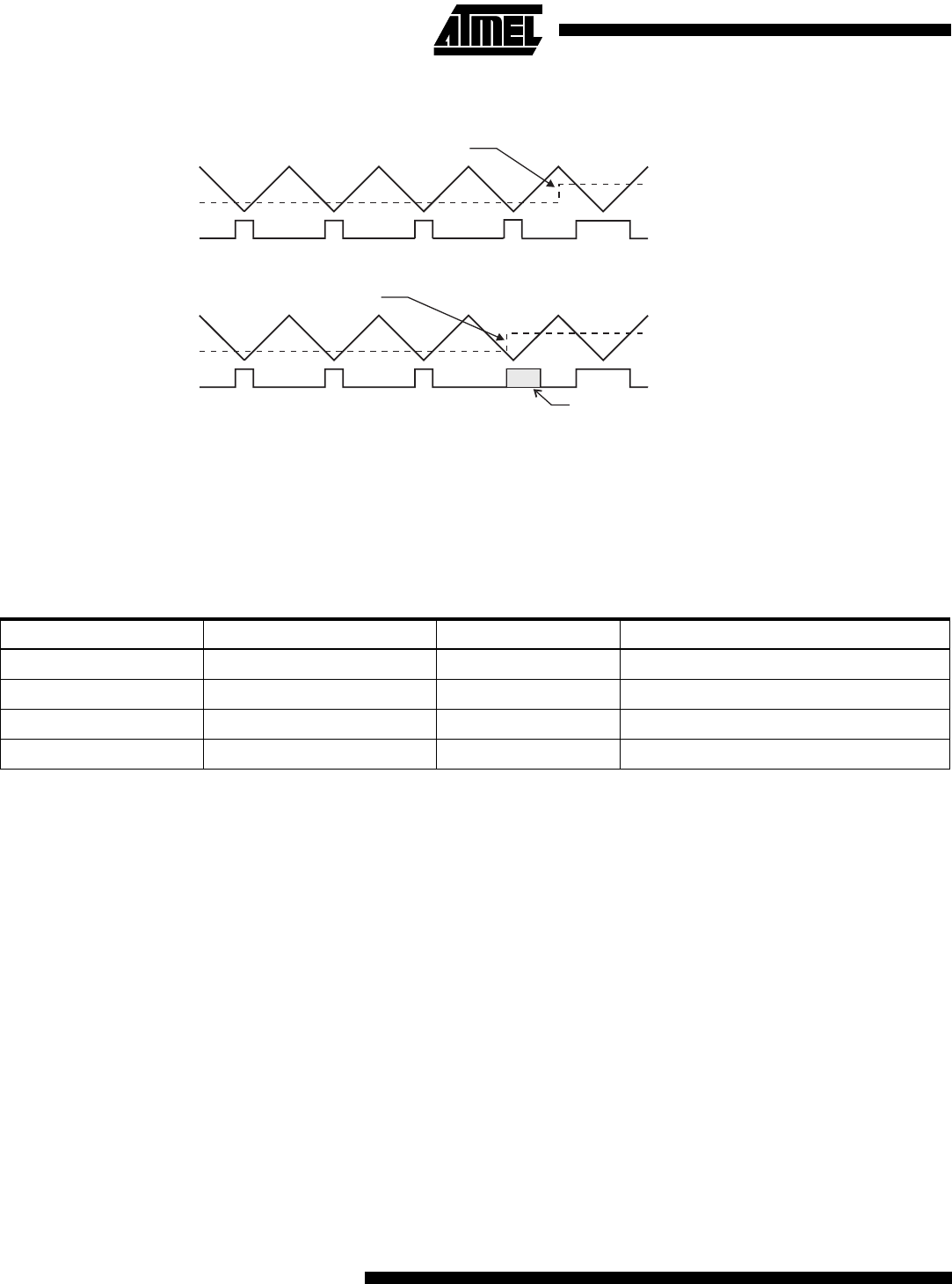
Figure 35. Effects on Unsynchronized OCR1 Latching
During the time between the write and the latch operation, a read from OCR1A or OCR1B will read the contents of the tem-
porary location. This means that the most recently written value always will read out of OCR1A/B
When the OCR1A/OCR1B contains $0000 or TOP, the output OC1A/OC1B is updated to low or high on the next compare
match according to the settings of COM1A1/COM1A0 or COM1B1/COM1B0. This is shown in Table 21.
Note: X = A or B
In PWM mode, the Timer Overflow Flag1, TOV1, is set when the counter advances from $0000. Timer Overflow Interrupt1
operates exactly as in normal Timer/Counter mode, i.e. it is executed when TOV1 is set provided that Timer Overflow
Interrupt1 and global interrupts are enabled. This does also apply to the Timer Output Compare1 flags and interrupts.
Table 21. PWM Outputs OCR1X = $0000 Or TOP
COM1X1 COM1X0 OCR1X Output OC1X
1 0 $0000 L
10TOP H
1 1 $0000 H
11TOP L
Counter
V
alue
Compare V
alue
PWM
Output OC1X
Synchronized OCR1X Latch
Counter
Value
Compare Value
PWM Output OC1X
Unsynchronized OCR1X Latch
Glitch
Compare Value changes
Note: X = A or B
Compare V
alue changes