
Manual


Table Of Contents
- Ordering Information
- Features
- Description
- Architectural Overview
- General Purpose Register File
- ALU - Arithmetic Logic Unit
- ISP Flash Program Memory
- SRAM Data Memory
- Program and Data Addressing Modes
- Register Direct, Single Register Rd
- Register Direct, Two Registers Rd and Rr
- I/O Direct
- Data Direct
- Data Indirect with Displacement
- Data Indirect
- Data Indirect With Pre-Decrement
- Data Indirect With Post-Increment
- Constant Addressing Using the LPM and ELPM Instructions
- Direct Program Address, JMP and CALL
- Indirect Program Addressing, IJMP and ICALL
- Relative Program Addressing, RJMP and RCALL
- EEPROM Data Memory
- Memory Access Times and Instruction Execution Timing
- I/O Memory
- Reset and Interrupt Handling
- Reset Sources
- Power-On Reset
- External Reset
- Watchdog Reset
- MCU Status Register - MCUSR
- Interrupt Handling
- External Interrupt Mask Register - EIMSK
- External Interrupt Flag Register - EIFR
- External Interrupt Control Register - EICR
- Timer/Counter Interrupt Mask Register - TIMSK
- Timer/Counter Interrupt Flag Register - TIFR
- Interrupt Response Time
- Sleep Modes
- Timer/Counters
- Timer/Counter Prescalers
- 8-bit Timer/Counters T/C0 and T/C2
- Timer/Counter0 Control Register - TCCR0
- Timer/Counter2 Control Register - TCCR2
- Timer/Counter0 - TCNT0
- Timer/Counter2 - TCNT2
- Timer/Counter0 Output Compare Register - OCR0
- Timer/Counter2 Output Compare Register - OCR2
- Timer/Counter 0 and 2 in PWM mode
- Asynchronous Status Register - ASSR
- Asynchronous Operation of Timer/Counter0
- 16-bit Timer/Counter1
- Timer/Counter1 Control Register A - TCCR1A
- Timer/Counter1 Control Register B - TCCR1B
- Timer/Counter1 - TCNT1H and TCNT1L
- Timer/Counter1 Output Compare Register - OCR1AH and OCR1AL
- Timer/Counter1 Output Compare Register - OCR1BH and OCR1BL
- Timer/Counter1 Input Capture Register - ICR1H and ICR1L
- Timer/Counter1 in PWM mode
- Watchdog Timer
- EEPROM Read/Write Access
- Serial Peripheral Interface - SPI
- UART
- Analog Comparator
- Analog to Digital Converter
- Interface to external SRAM
- I/O-Ports
- Memory Programming
- Electrical Characteristics
- Typical characteristics
- Register Summary
- Instruction Set Summary (Continued)
ATmega603/103
49
Since the Input Capture Register - ICR1 - is a 16-bit register, a temporary register TEMP is used when ICR1 is read to
ensure that both bytes are read simultaneously. When the CPU reads the low byte ICR1L, the data is sent to the CPU and
the data of the high byte ICR1H is placed in the TEMP register. When the CPU reads the data in the high byte ICR1H, the
CPU receives the data in the TEMP register. Consequently, the low byte ICR1L must be accessed first for a full 16-bit reg-
ister read operation.
The TEMP register is also used when accessing TCNT1, OCR1A and OCR1B. If the main program and also interrupt
routines perform access to registers using TEMP, interrupts must be disabled during access from the main program.
Timer/Counter1 in PWM mode
When the PWM mode is selected, Timer/Counter1 and the Output Compare Register1A - OCR1A and the Output Compare
Register1B - OCR1B, form a dual 8, 9 or 10-bit, free-running, glitch-free and phase correct PWM with outputs on the
PB5(OC1A) and PB6(OC1B) pins. Timer/Counter1 acts as an up/down counter, counting up from $0000 to TOP (see Table
17), where it turns and counts down again to zero before the cycle is repeated. When the counter value matches the con-
tents of the 10 least significant bits of OCR1A or OCR1B, the PB5(OC1A)/PB6(OC1B) pins are set or cleared according to
the settings of the COM1A1/COM1A0 or COM1B1/COM1B0 bits in the Timer/Counter1 Control Register TCCR1A. Refer to
Table 20 for details.
Note: X = A or B
Note that in the PWM mode, the 10 least significant OCR1A/OCR1B bits, when written, are transferred to a temporary loca-
tion. They are latched when Timer/Counter1 reaches the value TOP. This prevents the occurrence of odd-length PWM
pulses (glitches) in the event of an unsynchronized OCR1A/OCR1B write. See Figure 35 for an example.
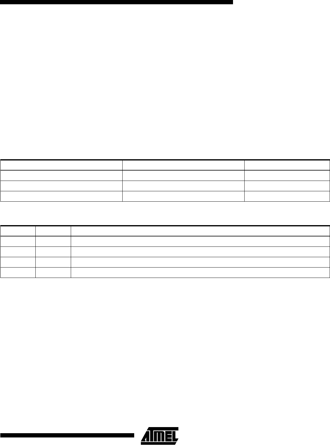
Table 19. Timer TOP Values and PWM Frequency
PWM Resolution Timer TOP value Frequency
8-bit $00FF (255) f
TCK1
/510
9-bit $01FF (511) f
TCK1
/1022
10-bit $03FF(1023) f
TCK1
/2046
Table 20. Compare1 Mode Select in PWM Mode
COM1X1 COM1X0 Effect on OCX1
0 0 Not connected
0 1 Not connected
1 0 Cleared on compare match, up-counting. Set on compare match, down-counting (non-inverted PWM).
1 1 Cleared on compare match, down-counting. Set on compare match, up-counting (inverted PWM).