
Manual


Table Of Contents
- Ordering Information
- Features
- Description
- Architectural Overview
- General Purpose Register File
- ALU - Arithmetic Logic Unit
- ISP Flash Program Memory
- SRAM Data Memory
- Program and Data Addressing Modes
- Register Direct, Single Register Rd
- Register Direct, Two Registers Rd and Rr
- I/O Direct
- Data Direct
- Data Indirect with Displacement
- Data Indirect
- Data Indirect With Pre-Decrement
- Data Indirect With Post-Increment
- Constant Addressing Using the LPM and ELPM Instructions
- Direct Program Address, JMP and CALL
- Indirect Program Addressing, IJMP and ICALL
- Relative Program Addressing, RJMP and RCALL
- EEPROM Data Memory
- Memory Access Times and Instruction Execution Timing
- I/O Memory
- Reset and Interrupt Handling
- Reset Sources
- Power-On Reset
- External Reset
- Watchdog Reset
- MCU Status Register - MCUSR
- Interrupt Handling
- External Interrupt Mask Register - EIMSK
- External Interrupt Flag Register - EIFR
- External Interrupt Control Register - EICR
- Timer/Counter Interrupt Mask Register - TIMSK
- Timer/Counter Interrupt Flag Register - TIFR
- Interrupt Response Time
- Sleep Modes
- Timer/Counters
- Timer/Counter Prescalers
- 8-bit Timer/Counters T/C0 and T/C2
- Timer/Counter0 Control Register - TCCR0
- Timer/Counter2 Control Register - TCCR2
- Timer/Counter0 - TCNT0
- Timer/Counter2 - TCNT2
- Timer/Counter0 Output Compare Register - OCR0
- Timer/Counter2 Output Compare Register - OCR2
- Timer/Counter 0 and 2 in PWM mode
- Asynchronous Status Register - ASSR
- Asynchronous Operation of Timer/Counter0
- 16-bit Timer/Counter1
- Timer/Counter1 Control Register A - TCCR1A
- Timer/Counter1 Control Register B - TCCR1B
- Timer/Counter1 - TCNT1H and TCNT1L
- Timer/Counter1 Output Compare Register - OCR1AH and OCR1AL
- Timer/Counter1 Output Compare Register - OCR1BH and OCR1BL
- Timer/Counter1 Input Capture Register - ICR1H and ICR1L
- Timer/Counter1 in PWM mode
- Watchdog Timer
- EEPROM Read/Write Access
- Serial Peripheral Interface - SPI
- UART
- Analog Comparator
- Analog to Digital Converter
- Interface to external SRAM
- I/O-Ports
- Memory Programming
- Electrical Characteristics
- Typical characteristics
- Register Summary
- Instruction Set Summary (Continued)
ATmega603/103
48
Timer/Counter1 Output Compare Register - OCR1AH and OCR1AL
Timer/Counter1 Output Compare Register - OCR1BH and OCR1BL
The output compare registers are 16-bit read/write registers.
The Timer/Counter1 Output Compare Registers contain the data to be continuously compared with Timer/Counter1.
Actions on compare matches are specified in the Timer/Counter1 Control and Status register. A compare match does only
occur if Timer/Counter1 counts to the OCR value. A software write that sets TCNT1 and OCR1A or OCR1B to the same
value does not generate a compare match.
A compare match will set the compare interrupt flag in the CPU clock cycle following the compare event.
Since the Output Compare Registers - OCR1A and OCR1B - are 16-bit registers, a temporary register TEMP is used when
OCR1A/B are written to ensure that both bytes are updated simultaneously. When the CPU writes the high byte, OCR1AH
or OCR1BH, the data is temporarily stored in the TEMP register. When the CPU writes the low byte, OCR1AL or OCR1BL,
the TEMP register is simultaneously written to OCR1AH or OCR1BH. Consequently, the high byte OCR1AH or OCR1BH
must be written first for a full 16-bit register write operation.
The TEMP register is also used when accessing TCNT1, and ICR1. If the main program and also interrupt routines perform
access to registers using TEMP, interrupts must be disabled during access from the main program.
Timer/Counter1 Input Capture Register - ICR1H and ICR1L
The input capture register is a 16-bit read-only register.
When the rising or falling edge (according to the input capture edge setting - ICES1) of the signal at the input capture pin -
PD4(IC1) - is detected, the current value of the Timer/Counter1 is transferred to the Input Capture Register - ICR1. At the
same time, the input capture flag - ICF1 - is set (one).
Bit 151413121110 9 8
$2B MSB OCR1AH
$2A LSB OCR1AL
76543210
Read/Write R/W R/W R/W R/W R/W R/W R/W R/W
R/W R/W R/W R/W R/W R/W R/W R/W
Initial value00000000
00000000
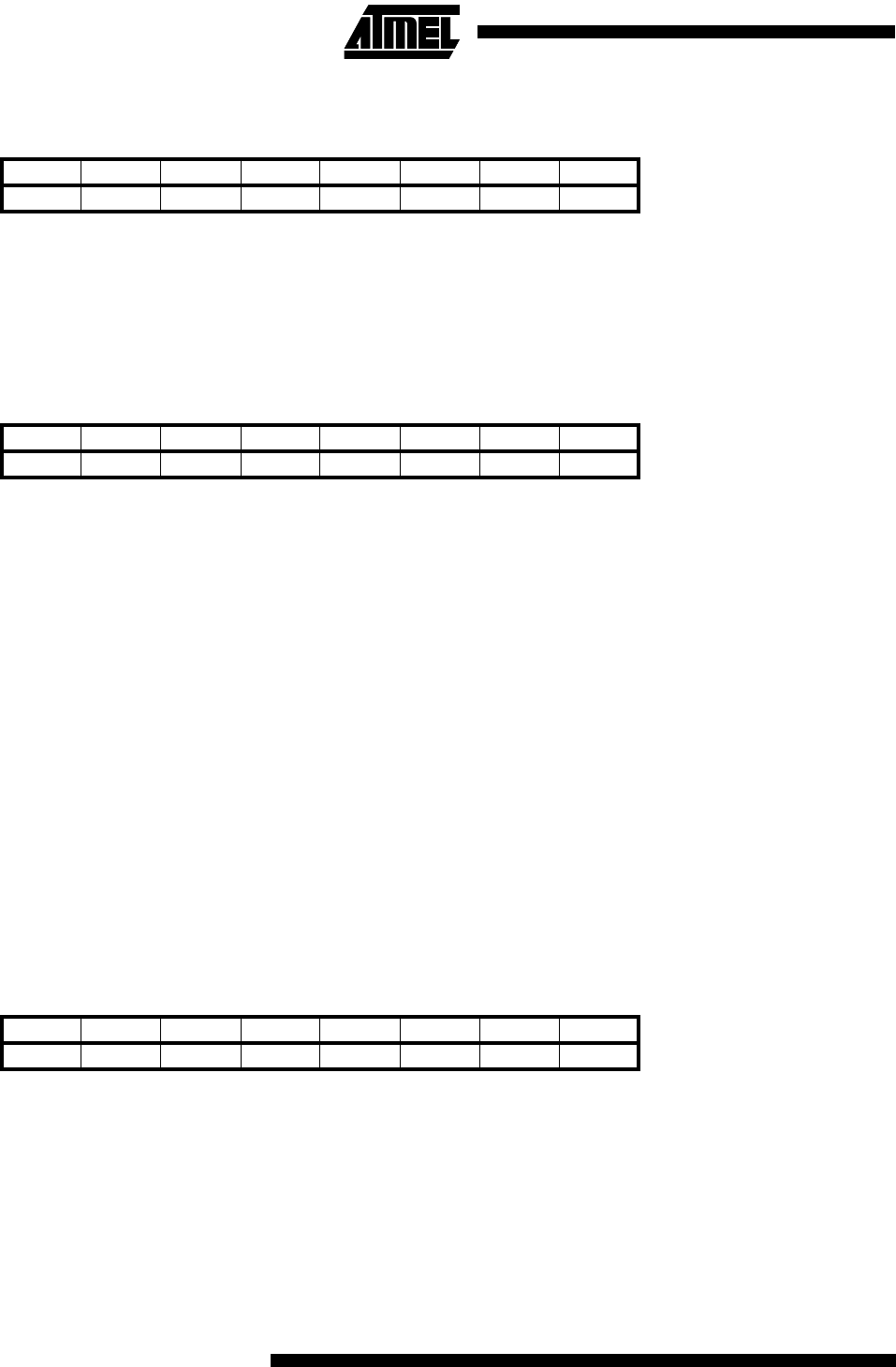
Bit 151413121110 9 8
$29 MSB OCR1BH
$28 LSB OCR1BL
76543210
Read/Write R/W R/W R/W R/W R/W R/W R/W R/W
R/W R/W R/W R/W R/W R/W R/W R/W
Initial value00000000
00000000
Bit 151413121110 9 8
$27 ($37) MSB ICR1H
$26 ($36) LSB ICR1L
76543210
Read/WriteRRRRRRRR
RRRRRRRR
Initial value00000000
00000000