
Manual


Table Of Contents
- Ordering Information
- Features
- Description
- Architectural Overview
- General Purpose Register File
- ALU - Arithmetic Logic Unit
- ISP Flash Program Memory
- SRAM Data Memory
- Program and Data Addressing Modes
- Register Direct, Single Register Rd
- Register Direct, Two Registers Rd and Rr
- I/O Direct
- Data Direct
- Data Indirect with Displacement
- Data Indirect
- Data Indirect With Pre-Decrement
- Data Indirect With Post-Increment
- Constant Addressing Using the LPM and ELPM Instructions
- Direct Program Address, JMP and CALL
- Indirect Program Addressing, IJMP and ICALL
- Relative Program Addressing, RJMP and RCALL
- EEPROM Data Memory
- Memory Access Times and Instruction Execution Timing
- I/O Memory
- Reset and Interrupt Handling
- Reset Sources
- Power-On Reset
- External Reset
- Watchdog Reset
- MCU Status Register - MCUSR
- Interrupt Handling
- External Interrupt Mask Register - EIMSK
- External Interrupt Flag Register - EIFR
- External Interrupt Control Register - EICR
- Timer/Counter Interrupt Mask Register - TIMSK
- Timer/Counter Interrupt Flag Register - TIFR
- Interrupt Response Time
- Sleep Modes
- Timer/Counters
- Timer/Counter Prescalers
- 8-bit Timer/Counters T/C0 and T/C2
- Timer/Counter0 Control Register - TCCR0
- Timer/Counter2 Control Register - TCCR2
- Timer/Counter0 - TCNT0
- Timer/Counter2 - TCNT2
- Timer/Counter0 Output Compare Register - OCR0
- Timer/Counter2 Output Compare Register - OCR2
- Timer/Counter 0 and 2 in PWM mode
- Asynchronous Status Register - ASSR
- Asynchronous Operation of Timer/Counter0
- 16-bit Timer/Counter1
- Timer/Counter1 Control Register A - TCCR1A
- Timer/Counter1 Control Register B - TCCR1B
- Timer/Counter1 - TCNT1H and TCNT1L
- Timer/Counter1 Output Compare Register - OCR1AH and OCR1AL
- Timer/Counter1 Output Compare Register - OCR1BH and OCR1BL
- Timer/Counter1 Input Capture Register - ICR1H and ICR1L
- Timer/Counter1 in PWM mode
- Watchdog Timer
- EEPROM Read/Write Access
- Serial Peripheral Interface - SPI
- UART
- Analog Comparator
- Analog to Digital Converter
- Interface to external SRAM
- I/O-Ports
- Memory Programming
- Electrical Characteristics
- Typical characteristics
- Register Summary
- Instruction Set Summary (Continued)
ATmega603/103
46
Timer/Counter1 Control Register B - TCCR1B
•
Bit 7 - ICNC1: Input Capture1 Noise Canceler (4 CKs)
When the ICNC1 bit is cleared (zero), the input capture trigger noise canceler function is disabled. The input capture is trig-
gered at the first rising/falling edge sampled on the input capture pin PD4(IC1) as specified. When the ICNC1 bit is set
(one), four successive samples are measures on PD4(IC1), and all samples must be high/low according to the input cap-
ture trigger specification in the ICES1 bit. The actual sampling frequency is XTAL clock frequency.
•
Bit 6 - ICES1: Input Capture1 Edge Select
While the ICES1 bit is cleared (zero), the Timer/Counter1 contents are transferred to the Input Capture Register - ICR1 - on
the falling edge of the input capture pin - PD4(IC1). While the ICES1 bit is set (one), the Timer/Counter1 contents are trans-
ferred to the Input Capture Register - ICR1 - on the rising edge of the input capture pin - PD4(IC1).
•
Bits 5, 4 - Res: Reserved bits
These bits are reserved bits in the ATmega603/103 and always read zero.
•
Bit 3 - CTC1: Clear Timer/Counter1 on Compare Match
When the CTC1 control bit is set (one), the Timer/Counter1 is reset to $0000 in the clock cycle after a compareA match. If
the CTC1 control bit is cleared, Timer/Counter1 continues counting and is unaffected by a compare match. Since the com-
pare match is detected in the CPU clock cycle following the match, this function will behave differently when a prescaling
higher than 1 is used for the timer. When a prescaling of 1 is used, and the compareA register is set to C, the timer will
count as follows i CTC1 is set:
... | C-2 | C-1 | C | 0 | 1 | ...
When the prescaler is set to divide by 8, the timer will count like this:
... | C-2, C-2, C-2, C-2, C-2, C-2, C-2, C-2 | C-1, C-1, C-1, C-1, C-1, C-1, C-1, C-1 | C, 0, 0, 0, 0, 0, 0, 0 | ...
In PWM mode, this bit has no effect.
•
Bits 2,1,0 - CS12, CS11, CS10: Clock Select1, bit 2,1 and 0
The lock Select1 bits 2,1 and 0 define the prescaling source of Timer/Counter1.
The Stop condition provides a Timer Enable/Disable function. The CK down divided modes are scaled directly from the CK
CPU clock. If the external pin modes are used for Timer/Counter1, transitions on PD6/(T1) will clock the counter even if the
pin is configured as an output. This feature can give the user SW control of the counting.
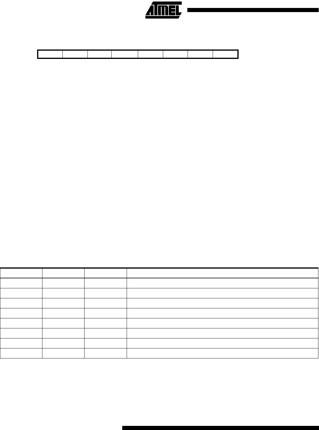
Bit 7 6 5 4 3 2 1 0
$2E ($4E) ICNC1 ICES1 - - CTC1 CS12 CS11 CS10 TCCR1B
Read/Write R/W R/W R R R/W R/W R/W R/W
Initial value 0 0 0 0 0 0 0 0
Table 18. Clock 1 Prescale Select
CS12 CS11 CS10 Description
0 0 0 Stop, the Timer/Counter1 is stopped.
001CK
010CK/8
011CK/64
100CK/256
101CK/1024
1 1 0 External Pin T1, falling edge
1 1 1 External Pin T1, rising edge