
Manual


Table Of Contents
- Ordering Information
- Features
- Description
- Architectural Overview
- General Purpose Register File
- ALU - Arithmetic Logic Unit
- ISP Flash Program Memory
- SRAM Data Memory
- Program and Data Addressing Modes
- Register Direct, Single Register Rd
- Register Direct, Two Registers Rd and Rr
- I/O Direct
- Data Direct
- Data Indirect with Displacement
- Data Indirect
- Data Indirect With Pre-Decrement
- Data Indirect With Post-Increment
- Constant Addressing Using the LPM and ELPM Instructions
- Direct Program Address, JMP and CALL
- Indirect Program Addressing, IJMP and ICALL
- Relative Program Addressing, RJMP and RCALL
- EEPROM Data Memory
- Memory Access Times and Instruction Execution Timing
- I/O Memory
- Reset and Interrupt Handling
- Reset Sources
- Power-On Reset
- External Reset
- Watchdog Reset
- MCU Status Register - MCUSR
- Interrupt Handling
- External Interrupt Mask Register - EIMSK
- External Interrupt Flag Register - EIFR
- External Interrupt Control Register - EICR
- Timer/Counter Interrupt Mask Register - TIMSK
- Timer/Counter Interrupt Flag Register - TIFR
- Interrupt Response Time
- Sleep Modes
- Timer/Counters
- Timer/Counter Prescalers
- 8-bit Timer/Counters T/C0 and T/C2
- Timer/Counter0 Control Register - TCCR0
- Timer/Counter2 Control Register - TCCR2
- Timer/Counter0 - TCNT0
- Timer/Counter2 - TCNT2
- Timer/Counter0 Output Compare Register - OCR0
- Timer/Counter2 Output Compare Register - OCR2
- Timer/Counter 0 and 2 in PWM mode
- Asynchronous Status Register - ASSR
- Asynchronous Operation of Timer/Counter0
- 16-bit Timer/Counter1
- Timer/Counter1 Control Register A - TCCR1A
- Timer/Counter1 Control Register B - TCCR1B
- Timer/Counter1 - TCNT1H and TCNT1L
- Timer/Counter1 Output Compare Register - OCR1AH and OCR1AL
- Timer/Counter1 Output Compare Register - OCR1BH and OCR1BL
- Timer/Counter1 Input Capture Register - ICR1H and ICR1L
- Timer/Counter1 in PWM mode
- Watchdog Timer
- EEPROM Read/Write Access
- Serial Peripheral Interface - SPI
- UART
- Analog Comparator
- Analog to Digital Converter
- Interface to external SRAM
- I/O-Ports
- Memory Programming
- Electrical Characteristics
- Typical characteristics
- Register Summary
- Instruction Set Summary (Continued)
ATmega603/103
45
If the noise canceler function is enabled, the actual trigger condition for the capture event is monitored over 4 samples, and
all 4 must be equal to activate the capture flag.
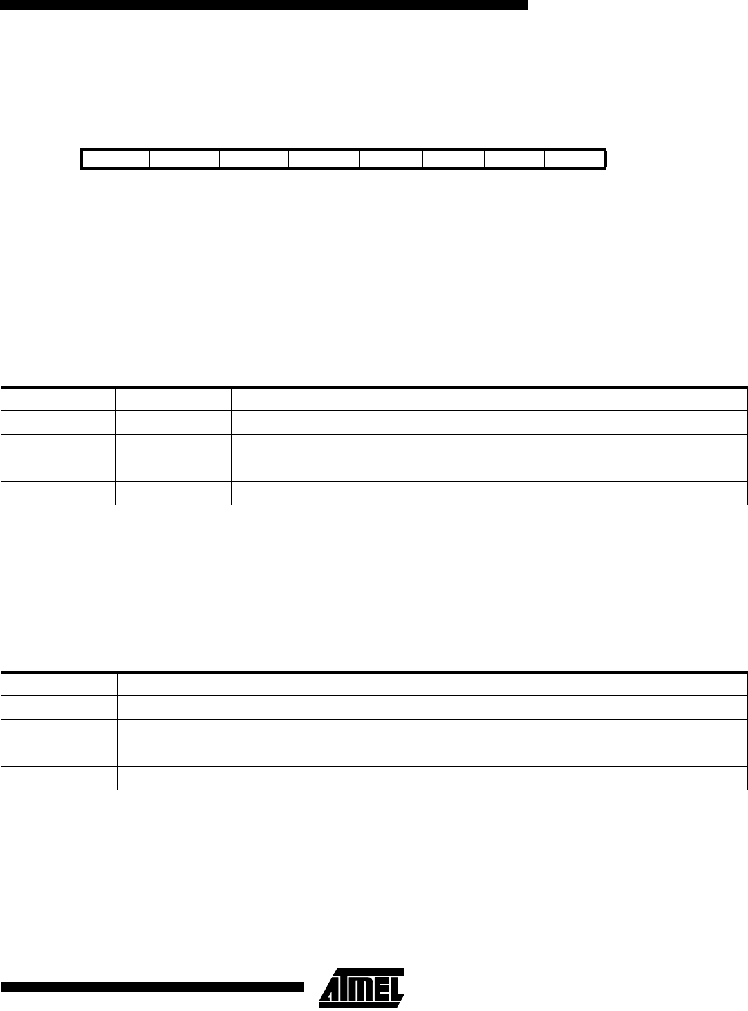
Timer/Counter1 Control Register A - TCCR1A
•
Bits 7..6 - COM1A1, COM1A0: Compare Output Mode1A, bits 1 and 0
The COM1A1 and COM1A0 control bits determine any output pin action following a compare match in Timer/Counter1.
Any output pin actions affect pin OC1A - Output CompareA pin 1. This is an alternative function to an I/O port, and the cor-
responding direction control bit must be set (one) to control an output pin. The control configuration is shown in Table 16..
•
Bits 5..4 - COM1B1, COM1B0: Compare Output Mode1B, bits 1 and 0
The COM1B1 and COM1B0 control bits determine any output pin action following a compare match in Timer/Counter1.
Any output pin actions affect pin OC1B - Output CompareB. Since this is an alternative function to an I/O port, the corre-
sponding direction control bit must be set (one) to control an output pin. The following control configuration is given:
Note: X = A or B.
In PWM mode, these bits have a different function. Refer to Table 17 for a detailed description.
• Bits 3..2 - Res: Reserved bits
These bits are reserved bits in the ATmega603/103 and always read zero.
•
Bits 1..0 - PWM11, PWM10: Pulse Width Modulator Select Bits
These bits select PWM operation of Timer/Counter1 as specified in Table 19. This mode is described on page 49.
Bit 7 6 5 4 3 2 1 0
$2F ($4F) COM1A1 COM1A0 COM1B1 COM1B0 - - PWM11 PWM10 TCCR1A
Read/Write R/W R/W R/W R/W R R R/W R/W
Initial value 0 0 0 0 0 0 0 0
Table 16. Compare 1 Mode Select
COM1X1 COM1X0 Description
0 0 Timer/Counter1 disconnected from output pin OC1X
0 1 Toggle the OC1X output line.
1 0 Clear the OC1X output line (to zero).
1 1 Set the OC1X output line (to one).
Table 17. PWM Mode Select
PWM11 PWM10 Description
0 0 PWM operation of Timer/Counter1 is disabled
0 1 Timer/Counter1 is an 8-bit PWM
1 0 Timer/Counter1 is a 9-bit PWM
1 1 Timer/Counter1 is a 10-bit PWM