
Manual


Table Of Contents
- Ordering Information
- Features
- Description
- Architectural Overview
- General Purpose Register File
- ALU - Arithmetic Logic Unit
- ISP Flash Program Memory
- SRAM Data Memory
- Program and Data Addressing Modes
- Register Direct, Single Register Rd
- Register Direct, Two Registers Rd and Rr
- I/O Direct
- Data Direct
- Data Indirect with Displacement
- Data Indirect
- Data Indirect With Pre-Decrement
- Data Indirect With Post-Increment
- Constant Addressing Using the LPM and ELPM Instructions
- Direct Program Address, JMP and CALL
- Indirect Program Addressing, IJMP and ICALL
- Relative Program Addressing, RJMP and RCALL
- EEPROM Data Memory
- Memory Access Times and Instruction Execution Timing
- I/O Memory
- Reset and Interrupt Handling
- Reset Sources
- Power-On Reset
- External Reset
- Watchdog Reset
- MCU Status Register - MCUSR
- Interrupt Handling
- External Interrupt Mask Register - EIMSK
- External Interrupt Flag Register - EIFR
- External Interrupt Control Register - EICR
- Timer/Counter Interrupt Mask Register - TIMSK
- Timer/Counter Interrupt Flag Register - TIFR
- Interrupt Response Time
- Sleep Modes
- Timer/Counters
- Timer/Counter Prescalers
- 8-bit Timer/Counters T/C0 and T/C2
- Timer/Counter0 Control Register - TCCR0
- Timer/Counter2 Control Register - TCCR2
- Timer/Counter0 - TCNT0
- Timer/Counter2 - TCNT2
- Timer/Counter0 Output Compare Register - OCR0
- Timer/Counter2 Output Compare Register - OCR2
- Timer/Counter 0 and 2 in PWM mode
- Asynchronous Status Register - ASSR
- Asynchronous Operation of Timer/Counter0
- 16-bit Timer/Counter1
- Timer/Counter1 Control Register A - TCCR1A
- Timer/Counter1 Control Register B - TCCR1B
- Timer/Counter1 - TCNT1H and TCNT1L
- Timer/Counter1 Output Compare Register - OCR1AH and OCR1AL
- Timer/Counter1 Output Compare Register - OCR1BH and OCR1BL
- Timer/Counter1 Input Capture Register - ICR1H and ICR1L
- Timer/Counter1 in PWM mode
- Watchdog Timer
- EEPROM Read/Write Access
- Serial Peripheral Interface - SPI
- UART
- Analog Comparator
- Analog to Digital Converter
- Interface to external SRAM
- I/O-Ports
- Memory Programming
- Electrical Characteristics
- Typical characteristics
- Register Summary
- Instruction Set Summary (Continued)
ATmega603/103
44
Figure 33. Timer/Counter1 Block Diagram
Timer/Counter1 can also be used as a 8, 9 or 10-bit Pulse With Modulator. In this mode the counter and the
OCR1A/OCR1B registers serve as a dual glitch-free stand-alone PWM with centered pulses. Refer to page 49 for a
detailed description on this function.
The Input Capture function of Timer/Counter1 provides a capture of the Timer/Counter1 contents to the Input Capture
Register - ICR1, triggered by an external event on the Input Capture Pin - PD4/(IC1). The actual capture event settings
are defined by the Timer/Counter1 Control Register - TCCR1B. In addition, the Analog Comparator can be set to trigger
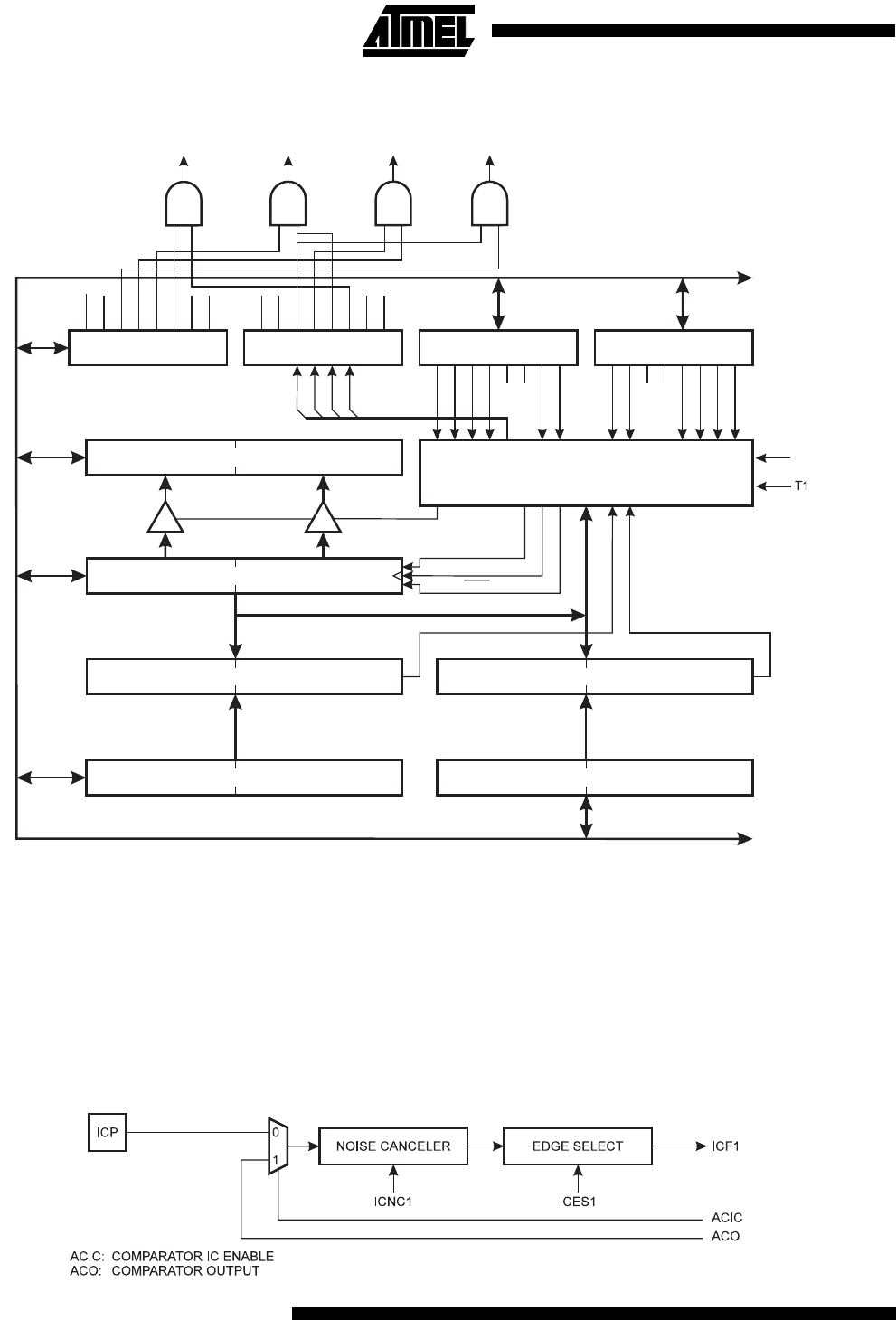
the Input Capture. Refer to the paragraph, “The Analog Comparator”, for details on this. The ICP pin logic is shown
in Figure 34.
Figure 34. ICP Pin Schematic Diagram
8-BIT DATA BUS
T/C1 CONTROL
REGISTER B (TCCR1B)
T/C1 CONTROL
REGISTER A (TCCR1A)
T/C1 INPUT CAPTURE REGISTER (ICR1)
16 BIT COMPARATOR
16 BIT COMPARATOR
TIMER/COUNTER1 OUTPUT COMPARE REGISTER A
TIMER/COUNTER1 OUTPUT COMPARE REGISTER B
TIMER/COUNTER1 (TCNT1)
TIMER INT. FLAG
REGISTER (TIFR)
0
0
0
0
0
0
7
7
7
7
7
7
8
8
8
8
8
8
15
15
15
15
15
15
CONTROL
LOGIC
COM1A1
COM1B1
CS12
TOV1
TOV1
OCF0
TOV0
OCF1A
OCF1A
OCF1B
OCF1B
ICF1
ICF1
COM1A0
COM1B0
CS11
CTC1
PWM11
PWM10
ICES1
ICNC1
CS10
C
K
T/C1 COMPARE
MATCHA IRQ
T/C1 COMPARE
MATCHB IRQ
T/C1 INPUT
CAPTURE IRQ
T/C1 OVER-
FLOW IRQ
CAPTURE
TRIGGER
T/C CLOCK SOURCE
T/C CLEAR
UP/DOWN
TIMER INT. MASK
REGISTER (TIMSK)
OCIE0
TOIE0
TOIE1
OCIE1A
OCIE1B
TICIE1
TOIE2
TOV2
OCIE2
OCF2