
Manual


Table Of Contents
- Ordering Information
- Features
- Description
- Architectural Overview
- General Purpose Register File
- ALU - Arithmetic Logic Unit
- ISP Flash Program Memory
- SRAM Data Memory
- Program and Data Addressing Modes
- Register Direct, Single Register Rd
- Register Direct, Two Registers Rd and Rr
- I/O Direct
- Data Direct
- Data Indirect with Displacement
- Data Indirect
- Data Indirect With Pre-Decrement
- Data Indirect With Post-Increment
- Constant Addressing Using the LPM and ELPM Instructions
- Direct Program Address, JMP and CALL
- Indirect Program Addressing, IJMP and ICALL
- Relative Program Addressing, RJMP and RCALL
- EEPROM Data Memory
- Memory Access Times and Instruction Execution Timing
- I/O Memory
- Reset and Interrupt Handling
- Reset Sources
- Power-On Reset
- External Reset
- Watchdog Reset
- MCU Status Register - MCUSR
- Interrupt Handling
- External Interrupt Mask Register - EIMSK
- External Interrupt Flag Register - EIFR
- External Interrupt Control Register - EICR
- Timer/Counter Interrupt Mask Register - TIMSK
- Timer/Counter Interrupt Flag Register - TIFR
- Interrupt Response Time
- Sleep Modes
- Timer/Counters
- Timer/Counter Prescalers
- 8-bit Timer/Counters T/C0 and T/C2
- Timer/Counter0 Control Register - TCCR0
- Timer/Counter2 Control Register - TCCR2
- Timer/Counter0 - TCNT0
- Timer/Counter2 - TCNT2
- Timer/Counter0 Output Compare Register - OCR0
- Timer/Counter2 Output Compare Register - OCR2
- Timer/Counter 0 and 2 in PWM mode
- Asynchronous Status Register - ASSR
- Asynchronous Operation of Timer/Counter0
- 16-bit Timer/Counter1
- Timer/Counter1 Control Register A - TCCR1A
- Timer/Counter1 Control Register B - TCCR1B
- Timer/Counter1 - TCNT1H and TCNT1L
- Timer/Counter1 Output Compare Register - OCR1AH and OCR1AL
- Timer/Counter1 Output Compare Register - OCR1BH and OCR1BL
- Timer/Counter1 Input Capture Register - ICR1H and ICR1L
- Timer/Counter1 in PWM mode
- Watchdog Timer
- EEPROM Read/Write Access
- Serial Peripheral Interface - SPI
- UART
- Analog Comparator
- Analog to Digital Converter
- Interface to external SRAM
- I/O-Ports
- Memory Programming
- Electrical Characteristics
- Typical characteristics
- Register Summary
- Instruction Set Summary (Continued)
ATmega603/103
41
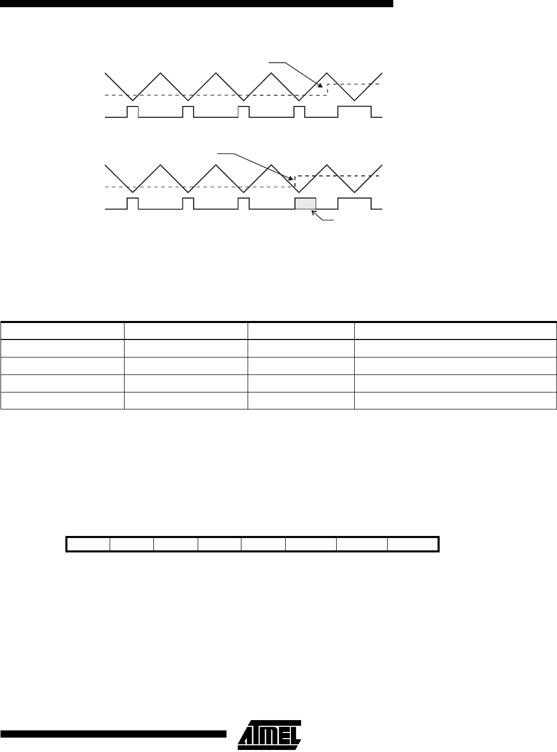
Figure 32. Effects on Unsynchronized OCR Latching
During the time between the write and the latch operation, a read from OCR0 or OCR2 will read the contents of the tempo-
rary location. This means that the most recently written value always will read out of OCR0/2
When the OCR register (not the temporary register) is updated to $00 or $FF, the PWM output changes to low or high
immediately according to the settings of COM21/COM20 or COM11/COM10. This is shown in Table 15:
Note: n = 0 or 2
In PWM mode, the Timer Overflow Flag, TOV0 or TOV2, is set when the counter advances from $00. Timer Overflow
Interrupt0 and 2 operates exactly as in normal Timer/Counter mode, i.e. it is executed when TOV0 or TOV2 is set provided
that Timer Overflow Interrupt and global interrupts are enabled. This does also apply to the Timer Output Compare flags
and interrupts.
The frequency of the PWM will be Timer Clock Frequency divided by 510.
Asynchronous Status Register - ASSR
•
Bit 7..4 - Res: Reserved Bits
These bits are reserved bits in the ATmega603/103 and always reads as zero.
•
Bit 3 - AS0: Asynchronous Timer/Counter0
When set(one) Timer/Counter0 is clocked from the TOSC1 pin. When cleared (zero) Timer/Counter0 is clocked from the
internal system clock, CK. When the value of this bit is changed the contents of TCNT0 might get corrupted.
•
Bit 2 - TCN0UB: Timer/Counter0 Update Busy
When Timer/Counter0 operates asynchronously and TCNT0 is written, this bit becomes set (one). When TCNT0 has been
updated from the temporary storage register, this bit is cleared (zero) by hardware. A logical zero in this bit indicates that
TCNT0 is ready to be updated with a new value.
Table 15. PWM Outputs OCRn = $00 or $FF
COMn1 COMn0 OCRn Output PWMn
1 0 $00 L
10$FF H
1 1 $00 H
11$FF L
Bit 76543 2 1 0
$30 ($50) - - - - AS0 TCN0UB OCR0UB TCR0UB ASSR
Read/Write R R R R R/W R R R
Initial value 0 0 0 0 0 0 0 0
Counter Value
Compare Value
PWM Output
Synchronized OCR Latch
Counter Value
Compare Value
PWM Output
Unsynchronized OCR Latch
Glitch
Compare Value changes
Compare Value changes