
Manual


Table Of Contents
- Ordering Information
- Features
- Description
- Architectural Overview
- General Purpose Register File
- ALU - Arithmetic Logic Unit
- ISP Flash Program Memory
- SRAM Data Memory
- Program and Data Addressing Modes
- Register Direct, Single Register Rd
- Register Direct, Two Registers Rd and Rr
- I/O Direct
- Data Direct
- Data Indirect with Displacement
- Data Indirect
- Data Indirect With Pre-Decrement
- Data Indirect With Post-Increment
- Constant Addressing Using the LPM and ELPM Instructions
- Direct Program Address, JMP and CALL
- Indirect Program Addressing, IJMP and ICALL
- Relative Program Addressing, RJMP and RCALL
- EEPROM Data Memory
- Memory Access Times and Instruction Execution Timing
- I/O Memory
- Reset and Interrupt Handling
- Reset Sources
- Power-On Reset
- External Reset
- Watchdog Reset
- MCU Status Register - MCUSR
- Interrupt Handling
- External Interrupt Mask Register - EIMSK
- External Interrupt Flag Register - EIFR
- External Interrupt Control Register - EICR
- Timer/Counter Interrupt Mask Register - TIMSK
- Timer/Counter Interrupt Flag Register - TIFR
- Interrupt Response Time
- Sleep Modes
- Timer/Counters
- Timer/Counter Prescalers
- 8-bit Timer/Counters T/C0 and T/C2
- Timer/Counter0 Control Register - TCCR0
- Timer/Counter2 Control Register - TCCR2
- Timer/Counter0 - TCNT0
- Timer/Counter2 - TCNT2
- Timer/Counter0 Output Compare Register - OCR0
- Timer/Counter2 Output Compare Register - OCR2
- Timer/Counter 0 and 2 in PWM mode
- Asynchronous Status Register - ASSR
- Asynchronous Operation of Timer/Counter0
- 16-bit Timer/Counter1
- Timer/Counter1 Control Register A - TCCR1A
- Timer/Counter1 Control Register B - TCCR1B
- Timer/Counter1 - TCNT1H and TCNT1L
- Timer/Counter1 Output Compare Register - OCR1AH and OCR1AL
- Timer/Counter1 Output Compare Register - OCR1BH and OCR1BL
- Timer/Counter1 Input Capture Register - ICR1H and ICR1L
- Timer/Counter1 in PWM mode
- Watchdog Timer
- EEPROM Read/Write Access
- Serial Peripheral Interface - SPI
- UART
- Analog Comparator
- Analog to Digital Converter
- Interface to external SRAM
- I/O-Ports
- Memory Programming
- Electrical Characteristics
- Typical characteristics
- Register Summary
- Instruction Set Summary (Continued)
ATmega603/103
40
Timer/Counter0 Output Compare Register - OCR0
Timer/Counter2 Output Compare Register - OCR2
The output compare registers are 8-bit read/write registers.
The Timer/Counter Output Compare Registers contain the data to be continuously compared with the Timer/Counter.
Actions on compare matches are specified in TCCR0 and TCCR2. A compare match does only occur if the Timer/Counter
counts to the OCR value. A software write that sets the Timer/Counter and Output Compare Register to the same value
does not generate a compare match.
A compare match will set the compare interrupt flag in the CPU clock cycle following the compare event.
Timer/Counter 0 and 2 in PWM mode
When the PWM mode is selected, the Timer/Counter and the Output Compare Register - OCR0 or OCR2 form an 8-bit,
free-running, glitch-free and phase correct PWM with outputs on the PB4(OC0/PWM0) or PB7(OC2/PWM2) pin. The
Timer/Counter acts as an up/down counter, counting up from $00 to $FF, where it turns and counts down again to zero
before the cycle is repeated. When the counter value matches the contents of the Output Compare register, the
PB4(OC0/PWM0) or PB7(OC2/PWM2) pin is set or cleared according to the settings of the COM01/COM00 or
COM21/COM20 bits in the Timer/Counter Control Registers TCCR0 and TCCR2. Refer to Table 14 for details.
Note: n = 0 or 2
Note that in PWM mode, the Output Compare register is transferred to a temporary location when written. The value is
latched when the Timer/Counter reaches $FF. This prevents the occurrence of odd-length PWM pulses (glitches) in the
event of an unsynchronized OCR0 or OCR2 write. See Figure 32 for an example.
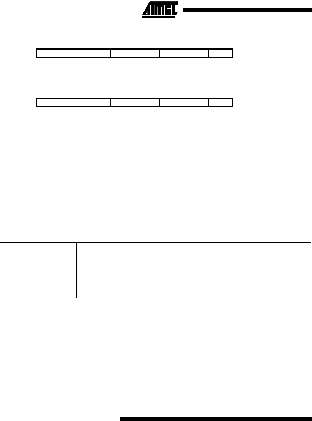
Bit 76543210
$31 ($51) MSB LSB OCR0
Read/Write R/W R/W R/W R/W R/W R/W R/W R/W
Initial value00000000
Bit 76543210
$23 ($43) MSB LSB OCR2
Read/Write R/W R/W R/W R/W R/W R/W R/W R/W
Initial value00000000
Table 14. Compare Mode Select in PWM Mode
COMn1 COMn0 Effect on Compare/PWM Pin
0 0 Not connected
0 1 Not connected
10
Cleared on compare match, up-counting. Set on compare match, down-counting (non-inverted
PWM).
1 1 Cleared on compare match, down-counting. Set on compare match, up-counting (inverted PWM).