
Manual


Table Of Contents
- Ordering Information
- Features
- Description
- Architectural Overview
- General Purpose Register File
- ALU - Arithmetic Logic Unit
- ISP Flash Program Memory
- SRAM Data Memory
- Program and Data Addressing Modes
- Register Direct, Single Register Rd
- Register Direct, Two Registers Rd and Rr
- I/O Direct
- Data Direct
- Data Indirect with Displacement
- Data Indirect
- Data Indirect With Pre-Decrement
- Data Indirect With Post-Increment
- Constant Addressing Using the LPM and ELPM Instructions
- Direct Program Address, JMP and CALL
- Indirect Program Addressing, IJMP and ICALL
- Relative Program Addressing, RJMP and RCALL
- EEPROM Data Memory
- Memory Access Times and Instruction Execution Timing
- I/O Memory
- Reset and Interrupt Handling
- Reset Sources
- Power-On Reset
- External Reset
- Watchdog Reset
- MCU Status Register - MCUSR
- Interrupt Handling
- External Interrupt Mask Register - EIMSK
- External Interrupt Flag Register - EIFR
- External Interrupt Control Register - EICR
- Timer/Counter Interrupt Mask Register - TIMSK
- Timer/Counter Interrupt Flag Register - TIFR
- Interrupt Response Time
- Sleep Modes
- Timer/Counters
- Timer/Counter Prescalers
- 8-bit Timer/Counters T/C0 and T/C2
- Timer/Counter0 Control Register - TCCR0
- Timer/Counter2 Control Register - TCCR2
- Timer/Counter0 - TCNT0
- Timer/Counter2 - TCNT2
- Timer/Counter0 Output Compare Register - OCR0
- Timer/Counter2 Output Compare Register - OCR2
- Timer/Counter 0 and 2 in PWM mode
- Asynchronous Status Register - ASSR
- Asynchronous Operation of Timer/Counter0
- 16-bit Timer/Counter1
- Timer/Counter1 Control Register A - TCCR1A
- Timer/Counter1 Control Register B - TCCR1B
- Timer/Counter1 - TCNT1H and TCNT1L
- Timer/Counter1 Output Compare Register - OCR1AH and OCR1AL
- Timer/Counter1 Output Compare Register - OCR1BH and OCR1BL
- Timer/Counter1 Input Capture Register - ICR1H and ICR1L
- Timer/Counter1 in PWM mode
- Watchdog Timer
- EEPROM Read/Write Access
- Serial Peripheral Interface - SPI
- UART
- Analog Comparator
- Analog to Digital Converter
- Interface to external SRAM
- I/O-Ports
- Memory Programming
- Electrical Characteristics
- Typical characteristics
- Register Summary
- Instruction Set Summary (Continued)
ATmega603/103
39
The Stop condition provides a Timer Enable/Disable function. The CK down divided modes are scaled directly from the CK
CPU clock. If the external pin modes are used for Timer/Counter2, transitions on PD7/(T2) will clock the counter even if the
pin is configured as an output. This feature can give the user SW control of the counting.
Timer/Counter0 - TCNT0
Timer/Counter2 - TCNT2
These 8-bit registers contains the value of the Timer/Counters.
Both Timer/Counters are realized as up or up/down (in PWM mode) counters with read and write access. If the
Timer/Counter is written to and a clock source is selected, it continues counting in the timer clock cycle after it is preset with
the written value.
Table 12. Timer/Counter0 Prescale Select
CS02 CS01 CS00 Description
0 0 0 Timer/Counter0 is stopped.
001PCK0
010PCK0/8
011PCK0/32
100PCK0/64
1 0 1 PCK0/128
1 1 0 PCK0/256
1 1 1 PCK0/1024
Table 13. Timer/Counter2 Prescale Select
CS22 CS21 CS20 Description
0 0 0 Timer/Counter2 is stopped.
001CK
0 1 0 CK/8
011CK/64
1 0 0 CK/256
1 0 1 CK/1024
1 1 0 External Pin PD7(T2), falling edge
1 1 1 External Pin PD7(T2), rising edge
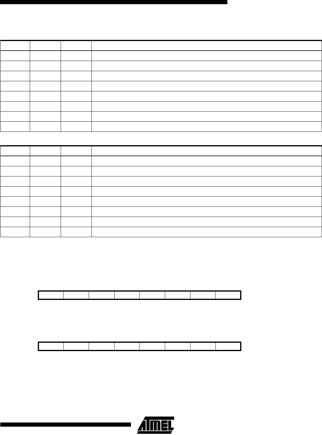
Bit 76543210
$32 ($42) MSB LSB TCNT0
Read/Write R/W R/W R/W R/W R/W R/W R/W R/W
Initial value00000000
Bit 76543210
$24 ($44) MSB LSB TCNT2
Read/Write R/W R/W R/W R/W R/W R/W R/W R/W
Initial value00000000