
Manual


Table Of Contents
- Ordering Information
- Features
- Description
- Architectural Overview
- General Purpose Register File
- ALU - Arithmetic Logic Unit
- ISP Flash Program Memory
- SRAM Data Memory
- Program and Data Addressing Modes
- Register Direct, Single Register Rd
- Register Direct, Two Registers Rd and Rr
- I/O Direct
- Data Direct
- Data Indirect with Displacement
- Data Indirect
- Data Indirect With Pre-Decrement
- Data Indirect With Post-Increment
- Constant Addressing Using the LPM and ELPM Instructions
- Direct Program Address, JMP and CALL
- Indirect Program Addressing, IJMP and ICALL
- Relative Program Addressing, RJMP and RCALL
- EEPROM Data Memory
- Memory Access Times and Instruction Execution Timing
- I/O Memory
- Reset and Interrupt Handling
- Reset Sources
- Power-On Reset
- External Reset
- Watchdog Reset
- MCU Status Register - MCUSR
- Interrupt Handling
- External Interrupt Mask Register - EIMSK
- External Interrupt Flag Register - EIFR
- External Interrupt Control Register - EICR
- Timer/Counter Interrupt Mask Register - TIMSK
- Timer/Counter Interrupt Flag Register - TIFR
- Interrupt Response Time
- Sleep Modes
- Timer/Counters
- Timer/Counter Prescalers
- 8-bit Timer/Counters T/C0 and T/C2
- Timer/Counter0 Control Register - TCCR0
- Timer/Counter2 Control Register - TCCR2
- Timer/Counter0 - TCNT0
- Timer/Counter2 - TCNT2
- Timer/Counter0 Output Compare Register - OCR0
- Timer/Counter2 Output Compare Register - OCR2
- Timer/Counter 0 and 2 in PWM mode
- Asynchronous Status Register - ASSR
- Asynchronous Operation of Timer/Counter0
- 16-bit Timer/Counter1
- Timer/Counter1 Control Register A - TCCR1A
- Timer/Counter1 Control Register B - TCCR1B
- Timer/Counter1 - TCNT1H and TCNT1L
- Timer/Counter1 Output Compare Register - OCR1AH and OCR1AL
- Timer/Counter1 Output Compare Register - OCR1BH and OCR1BL
- Timer/Counter1 Input Capture Register - ICR1H and ICR1L
- Timer/Counter1 in PWM mode
- Watchdog Timer
- EEPROM Read/Write Access
- Serial Peripheral Interface - SPI
- UART
- Analog Comparator
- Analog to Digital Converter
- Interface to external SRAM
- I/O-Ports
- Memory Programming
- Electrical Characteristics
- Typical characteristics
- Register Summary
- Instruction Set Summary (Continued)
ATmega603/103
38
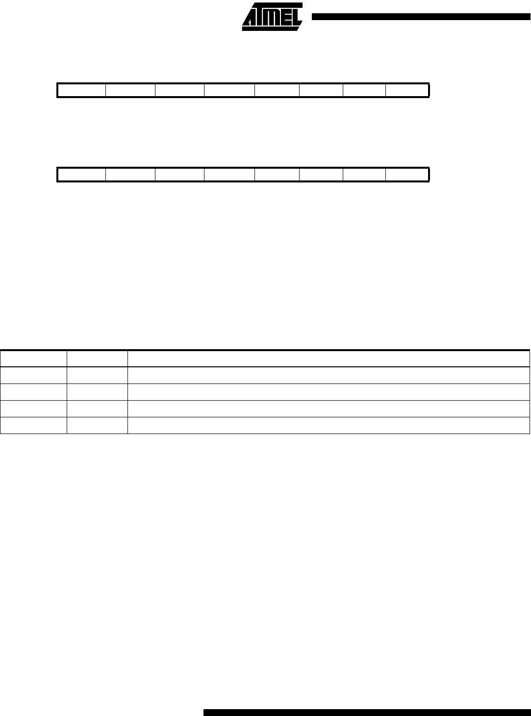
Timer/Counter0 Control Register - TCCR0
Timer/Counter2 Control Register - TCCR2
•
Bit 7 - Res: Reserved Bit
This bit is a reserved bit in the ATmega603/103 and always reads as zero.
•
Bit 6 - PWM0 / PWM2: Pulse Width Modulator Enable
When set (one) this bit enables PWM mode for Timer/Counter0 or Timer/Counter2. This mode is described on page 40.
•
Bits 5,4 - COM01, COM00 / COM21, COM20: Compare Output Mode, bits 1 and 0
The COMn1 and COMn0 control bits determine any output pin action following a compare match in Timer/Counter2.
Any output pin actions affect pins PB4(OC0/PWM0) or PB7(OC2/PWM2). Since this is an alternative function to an I/O
port, the corresponding direction control bit must be set (one) to control an output pin. The control configuration is shown in
Table 11.
Note: n = 0 or 2
In PWM mode, these bits have a different function. Refer to Table 14 for a detailed description.
• Bit 3 - CTC0 / CTC2: Clear Timer/Counter on Compare match
When the CTC0 or CTC2 control bit is set (one), the Timer/Counter is reset to $00 in the CPU clock cycle after a compare
match. If the control bit is cleared, the Timer continues counting and is unaffected by a compare match. Since the compare
match is detected in the CPU clock cycle following the match, this function will behave differently when a prescaling higher
than 1 is used for the timer. When a prescaling of 1 is used, and the compare register is set to C, the timer will count as fol-
lows if CTC0/2 is set:
... | C-2 | C-1 | C | 0 | 1 | ...
When the prescaler is set to divide by 8, the timer will count like this:
... | C-2, C-2, C-2, C-2, C-2, C-2, C-2, C-2 | C-1, C-1, C-1, C-1, C-1, C-1, C-1, C-1 | C, 0, 0, 0, 0, 0, 0, 0, 0 | 1, 1, 1, ...
In PWM mode, this bit has no effect.
•
Bits 2,1,0 - CS02, CS01, CS00 / CS22, CS21, CS20: Clock Select bits 2,1 and 0
The Clock Select2 bits 2,1 and 0 define the prescaling source of the Timer/Counter.
Bit 7 6 5 4 3 2 1 0
33 ($53) - PWM0 COM01 COM00 CTC0 CS02 CS01 CS00 TCCR0
Read/Write R R/W R/W R/W R/W R/W R/W R/W
Initial value 0 0 0 0 0 0 0 0
Bit 7 6 5 4 3 2 1 0
$25 ($45) - PWM2 COM21 COM20 CTC2 CS22 CS21 CS20 TCCR2
Read/Write R R/W R/W R/W R/W R/W R/W R/W
Initial value 0 0 0 0 0 0 0 0
Table 11. Compare Mode Select
COMn1 COMn0 Description
0 0 Timer/Counter disconnected from output pin OCn/PWMn
0 1 Toggle the OCn/PWMn output line.
1 0 Clear the OCn/PWMn output line (to zero).
1 1 Set the OCn/PWMn output line (to one).