
Manual


Table Of Contents
- Ordering Information
- Features
- Description
- Architectural Overview
- General Purpose Register File
- ALU - Arithmetic Logic Unit
- ISP Flash Program Memory
- SRAM Data Memory
- Program and Data Addressing Modes
- Register Direct, Single Register Rd
- Register Direct, Two Registers Rd and Rr
- I/O Direct
- Data Direct
- Data Indirect with Displacement
- Data Indirect
- Data Indirect With Pre-Decrement
- Data Indirect With Post-Increment
- Constant Addressing Using the LPM and ELPM Instructions
- Direct Program Address, JMP and CALL
- Indirect Program Addressing, IJMP and ICALL
- Relative Program Addressing, RJMP and RCALL
- EEPROM Data Memory
- Memory Access Times and Instruction Execution Timing
- I/O Memory
- Reset and Interrupt Handling
- Reset Sources
- Power-On Reset
- External Reset
- Watchdog Reset
- MCU Status Register - MCUSR
- Interrupt Handling
- External Interrupt Mask Register - EIMSK
- External Interrupt Flag Register - EIFR
- External Interrupt Control Register - EICR
- Timer/Counter Interrupt Mask Register - TIMSK
- Timer/Counter Interrupt Flag Register - TIFR
- Interrupt Response Time
- Sleep Modes
- Timer/Counters
- Timer/Counter Prescalers
- 8-bit Timer/Counters T/C0 and T/C2
- Timer/Counter0 Control Register - TCCR0
- Timer/Counter2 Control Register - TCCR2
- Timer/Counter0 - TCNT0
- Timer/Counter2 - TCNT2
- Timer/Counter0 Output Compare Register - OCR0
- Timer/Counter2 Output Compare Register - OCR2
- Timer/Counter 0 and 2 in PWM mode
- Asynchronous Status Register - ASSR
- Asynchronous Operation of Timer/Counter0
- 16-bit Timer/Counter1
- Timer/Counter1 Control Register A - TCCR1A
- Timer/Counter1 Control Register B - TCCR1B
- Timer/Counter1 - TCNT1H and TCNT1L
- Timer/Counter1 Output Compare Register - OCR1AH and OCR1AL
- Timer/Counter1 Output Compare Register - OCR1BH and OCR1BL
- Timer/Counter1 Input Capture Register - ICR1H and ICR1L
- Timer/Counter1 in PWM mode
- Watchdog Timer
- EEPROM Read/Write Access
- Serial Peripheral Interface - SPI
- UART
- Analog Comparator
- Analog to Digital Converter
- Interface to external SRAM
- I/O-Ports
- Memory Programming
- Electrical Characteristics
- Typical characteristics
- Register Summary
- Instruction Set Summary (Continued)
ATmega603/103
37
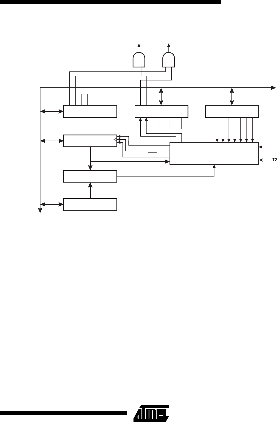
Figure 31. Timer/Counter2 Block Diagram
Note: Figure 31 shows the block diagram for Timer/Counter2.
The 8-bit Timer/Counter0 can select clock source from PCK0 or prescaled PCK0. The 8-bit Timer/Counter2 can select
clock source from CK, prescaled CK, or an external pin. Both Timer/Counters can be stopped as described in the specifica-
tion for the Timer/Counter Control Registers - TCCR0 and TCCR2.
The different status flags (overflow, compare match and capture event) are found in the Timer/Counter Interrupt Flag Reg-
ister - TIFR. Control signals are found in the Timer/Counter Control Registers - TCCR0 and TCCR2. The interrupt
enable/disable settings are found in the Timer/Counter Interrupt Mask Register - TIMSK.
When Timer/Counter2 is externally clocked, the external signal is synchronized with the oscillator frequency of the CPU. To
assure proper sampling of the external clock, the minimum time between two external clock transitions must be at least one
internal CPU clock period. The external clock signal is sampled on the rising edge of the internal CPU clock.
The 8-bit Timer/Counters feature a high resolution and a high accuracy usage with the lower prescaling opportunities. Sim-
ilarly, the high prescaling opportunities make these units useful for lower speed functions or exact timing functions with
infrequent actions.
Both Timer/Counters support two Output Compare functions using the Output Compare Registers - OCR0 and OCR2 as
the data source to be compared to the Timer/Counter contents. The Output Compare functions include optional clearing of
the counter on compare match, and action on the Output Compare Pins - PB4(OC0/PWM0) and PB7(OC2/PWM2) - on
compare match.
Timer/Counter0 and 2 can also be used as 8-bit Pulse Width Modulators. In this mode the Timer/Counter and the output
compare register serve as a glitch-free, stand-alone PWM with centered pulses. Refer to page 40 for a detailed description
on this function.
8-BIT DATA BUS
T/C2 CONTROL
REGISTER (TCCR2)
TIMER INT. FLAG
REGISTER (TIFR)
TIMER/COUNTER2
(TCNT2)
8-BIT COMPARATOR
OUTPUT COMPARE
REGISTER2 (OCR2)
TIMER INT. MASK
REGISTER (TIMSK)
0
0
0
7
7
7
T/C CLK SOURCE
UP/DOWN
T/C CLEAR
CONTROL
LOGIC
CS22
COM21
PWM2
OCF0
TOV0
TOV1
OCF2A
OCF2B
ICF1
TOV2
OCF2
OCF2
TOV2
OCIE0
TOIE0
TOIE1
OCIE1A
OCIE1B
TICIE1
TOIE2
OCIE2
CS21
COM20
CS20
CTC2
CK
T/C2 OVER-
FLOW IRQ
T/C2 COMPARE
MATCH IRQ