
Manual


Table Of Contents
- Ordering Information
- Features
- Description
- Architectural Overview
- General Purpose Register File
- ALU - Arithmetic Logic Unit
- ISP Flash Program Memory
- SRAM Data Memory
- Program and Data Addressing Modes
- Register Direct, Single Register Rd
- Register Direct, Two Registers Rd and Rr
- I/O Direct
- Data Direct
- Data Indirect with Displacement
- Data Indirect
- Data Indirect With Pre-Decrement
- Data Indirect With Post-Increment
- Constant Addressing Using the LPM and ELPM Instructions
- Direct Program Address, JMP and CALL
- Indirect Program Addressing, IJMP and ICALL
- Relative Program Addressing, RJMP and RCALL
- EEPROM Data Memory
- Memory Access Times and Instruction Execution Timing
- I/O Memory
- Reset and Interrupt Handling
- Reset Sources
- Power-On Reset
- External Reset
- Watchdog Reset
- MCU Status Register - MCUSR
- Interrupt Handling
- External Interrupt Mask Register - EIMSK
- External Interrupt Flag Register - EIFR
- External Interrupt Control Register - EICR
- Timer/Counter Interrupt Mask Register - TIMSK
- Timer/Counter Interrupt Flag Register - TIFR
- Interrupt Response Time
- Sleep Modes
- Timer/Counters
- Timer/Counter Prescalers
- 8-bit Timer/Counters T/C0 and T/C2
- Timer/Counter0 Control Register - TCCR0
- Timer/Counter2 Control Register - TCCR2
- Timer/Counter0 - TCNT0
- Timer/Counter2 - TCNT2
- Timer/Counter0 Output Compare Register - OCR0
- Timer/Counter2 Output Compare Register - OCR2
- Timer/Counter 0 and 2 in PWM mode
- Asynchronous Status Register - ASSR
- Asynchronous Operation of Timer/Counter0
- 16-bit Timer/Counter1
- Timer/Counter1 Control Register A - TCCR1A
- Timer/Counter1 Control Register B - TCCR1B
- Timer/Counter1 - TCNT1H and TCNT1L
- Timer/Counter1 Output Compare Register - OCR1AH and OCR1AL
- Timer/Counter1 Output Compare Register - OCR1BH and OCR1BL
- Timer/Counter1 Input Capture Register - ICR1H and ICR1L
- Timer/Counter1 in PWM mode
- Watchdog Timer
- EEPROM Read/Write Access
- Serial Peripheral Interface - SPI
- UART
- Analog Comparator
- Analog to Digital Converter
- Interface to external SRAM
- I/O-Ports
- Memory Programming
- Electrical Characteristics
- Typical characteristics
- Register Summary
- Instruction Set Summary (Continued)
ATmega603/103
36
The clock source for Timer/Counter0 prescaler is named PCK0. PCK0 is by default connected to the main system clock
CK. Observe that CPU clock frequency can be lower than the XTAL frequency if the XTAL divider is enabled. By setting the
AS0 bit in ASSR, Timer/Counter 0 prescaler is asynchronously clocked from the TOSC1 pin. This enables use of
Timer/Counter0 as a Real Time Clock (RTC). A crystal can be connected between the TOSC1 and TOSC2 pins to serve as
an independent clock source for Timer/Counter0. This oscillator is optimized for use with a 32.768 kHz crystal.
8-bit Timer/Counters T/C0 and T/C2
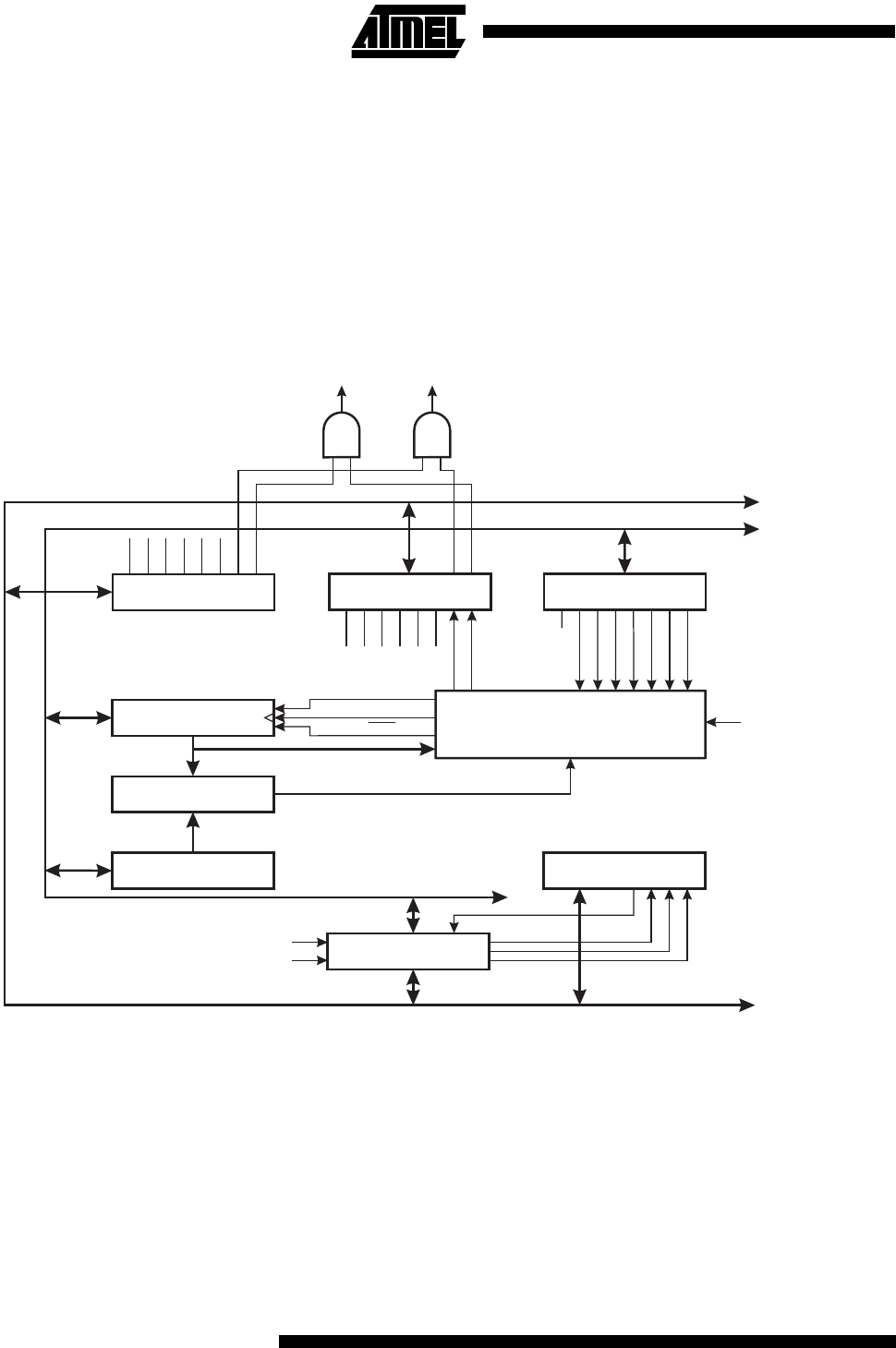
Figure 30 shows the block diagram for Timer/Counter0.
Figure 30. Timer/Counter0 Block Diagram
8-BIT DATA BUS
8-BIT ASYNCH T/C0 DATA BUS
ASYNCH. STATUS
REGISTER (ASSR)
TIMER INT. FLAG
REGISTER (TIFR)
TIMER/COUNTER0
(TCNT0)
SYNCH UNIT
8-BIT COMPARATOR
OUTPUT COMPARE
REGISTER0 (OCR0)
TIMER INT. MASK
REGISTER (TIMSK)
0
0
0
7
7
7
T/C CLK SOURCE
UP/DOWN
T/C CLEAR
CONTROL
LOGIC
OCF0
TOV0
TOV1
OCF2A
OCF2B
ICF1
TOV2
OCF2
OCF0
TOV0
OCIE0
TOIE0
TOIE1
OCIE1A
OCIE1B
TICIE1
TOIE2
OCIE2
OCR0UB
TC0UB
ICR0UB
PCK0
CK
TCK0
T/C0 OVER-
FLOW IRQ
T/C0 COMPARE
MATCH IRQ
T/C0 CONTROL
REGISTER (TCCR0)
CS02
COM01
PWM0
AS0
CS01
COM00
CS00
CTC0