
Manual


Table Of Contents
- Ordering Information
- Features
- Description
- Architectural Overview
- General Purpose Register File
- ALU - Arithmetic Logic Unit
- ISP Flash Program Memory
- SRAM Data Memory
- Program and Data Addressing Modes
- Register Direct, Single Register Rd
- Register Direct, Two Registers Rd and Rr
- I/O Direct
- Data Direct
- Data Indirect with Displacement
- Data Indirect
- Data Indirect With Pre-Decrement
- Data Indirect With Post-Increment
- Constant Addressing Using the LPM and ELPM Instructions
- Direct Program Address, JMP and CALL
- Indirect Program Addressing, IJMP and ICALL
- Relative Program Addressing, RJMP and RCALL
- EEPROM Data Memory
- Memory Access Times and Instruction Execution Timing
- I/O Memory
- Reset and Interrupt Handling
- Reset Sources
- Power-On Reset
- External Reset
- Watchdog Reset
- MCU Status Register - MCUSR
- Interrupt Handling
- External Interrupt Mask Register - EIMSK
- External Interrupt Flag Register - EIFR
- External Interrupt Control Register - EICR
- Timer/Counter Interrupt Mask Register - TIMSK
- Timer/Counter Interrupt Flag Register - TIFR
- Interrupt Response Time
- Sleep Modes
- Timer/Counters
- Timer/Counter Prescalers
- 8-bit Timer/Counters T/C0 and T/C2
- Timer/Counter0 Control Register - TCCR0
- Timer/Counter2 Control Register - TCCR2
- Timer/Counter0 - TCNT0
- Timer/Counter2 - TCNT2
- Timer/Counter0 Output Compare Register - OCR0
- Timer/Counter2 Output Compare Register - OCR2
- Timer/Counter 0 and 2 in PWM mode
- Asynchronous Status Register - ASSR
- Asynchronous Operation of Timer/Counter0
- 16-bit Timer/Counter1
- Timer/Counter1 Control Register A - TCCR1A
- Timer/Counter1 Control Register B - TCCR1B
- Timer/Counter1 - TCNT1H and TCNT1L
- Timer/Counter1 Output Compare Register - OCR1AH and OCR1AL
- Timer/Counter1 Output Compare Register - OCR1BH and OCR1BL
- Timer/Counter1 Input Capture Register - ICR1H and ICR1L
- Timer/Counter1 in PWM mode
- Watchdog Timer
- EEPROM Read/Write Access
- Serial Peripheral Interface - SPI
- UART
- Analog Comparator
- Analog to Digital Converter
- Interface to external SRAM
- I/O-Ports
- Memory Programming
- Electrical Characteristics
- Typical characteristics
- Register Summary
- Instruction Set Summary (Continued)
ATmega603/103
32
•
Bit 3 - OCIE1B: Timer/Counter1 Output CompareB Match Interrupt Enable
When the OCIE1B bit is set (one) and the I-bit in the Status Register is set (one), the Timer/Counter1 CompareB Match
interrupt is enabled. The corresponding interrupt (at vector $001A) is executed if a CompareB match in Timer/Counter1
occurs, i.e., when the OCF1B bit is set in the Timer/Counter Interrupt Flag Register - TIFR.
•
Bit 2 - TOIE1: Timer/Counter1 Overflow Interrupt Enable
When the TOIE1 bit is set (one) and the I-bit in the Status Register is set (one), the Timer/Counter1 Overflow interrupt is
enabled. The corresponding interrupt (at vector $001C) is executed if an overflow in Timer/Counter1 occurs, i.e., when the
TOV1 bit is set in the Timer/Counter Interrupt Flag Register - TIFR.
•
Bit 1 - OCIE0: Timer/Counter0 Output Compare Interrupt Enable
When the OCIE0 bit is set (one) and the I-bit in the Status Register is set (one), the Timer/Counter0 Compare Match inter-
rupt is enabled. The corresponding interrupt (at vector $001E) is executed if a Compare match in Timer/Counter0 occurs,
i.e., when the OCF0 bit is set in the Timer/Counter Interrupt Flag Register - TIFR.
•
Bit 0 - TOIE0: Timer/Counter0 Overflow Interrupt Enable
When the TOIE0 bit is set (one) and the I-bit in the Status Register is set (one), the Timer/Counter0 Overflow interrupt is
enabled. The corresponding interrupt (at vector $0020) is executed if an overflow in Timer/Counter0 occurs, i.e., when the
TOV0 bit is set in the Timer/Counter Interrupt Flag Register - TIFR
Timer/Counter Interrupt Flag Register - TIFR
•
Bit 7 - OCF2: Output Compare Flag 2:
The OCF2 bit is set (one) when compare match occurs between Timer/Counter2 and the data in OCR2 - Output Compare
Register 2. OCF2 is cleared by hardware when executing the corresponding interrupt handling vector. Alternatively, OCF2
is cleared by writing a logic one to the flag. When the I-bit in SREG, and OCIE2 (Timer/Counter2 Compare Interrupt
Enable), and the OCF2 are set (one), the Timer/Counter2 Output Compare Interrupt is executed.
•
Bit 6 - TOV2: Timer/Counter2 Overflow Flag
The TOV2 bit is set (one) when an overflow occurs in Timer/Counter2. TOV2 is cleared by hardware when executing the
corresponding interrupt handling vector. Alternatively, TOV2 is cleared by writing a logic one to the flag. When the I-bit in
SREG, and TOIE2 (Timer/Counter1 Overflow Interrupt Enable), and TOV2 are set (one), the Timer/Counter2 Overflow
Interrupt is executed. In PWM mode, this bit is set when Timer/Counter2 advances from $00.
•
Bit 5 - ICF1: Input Capture Flag 1
The ICF1 bit is set (one) to flag an input capture event, indicating that the Timer/Counter1 value has been transferred to the
input capture register - ICR1. ICF1 is cleared by hardware when executing the corresponding interrupt handling vector.
Alternatively, ICF1 is cleared by writing a logic one to the flag. When the SREG I-bit, and TICIE1 (Timer/Counter1 Input
Capture Interrupt Enable), and ICF1 are set (one), the Timer/Counter1 Capture Interrupt is executed.
•
Bit 4 - OCF1A: Output Compare Flag 1A
The OCF1A bit is set (one) when compare match occurs between the Timer/Counter1 and the data in OCR1A - Output
Compare Register 1A. OCF1A is cleared by hardware when executing the corresponding interrupt handling vector. Alterna-
tively, OCF1A is cleared by writing a logic one to the flag. When the I-bit in SREG, and OCIE1A (Timer/Counter1 Compare
Interrupt Enable), and the OCF1A are set (one), the Timer/Counter1 Compare A match Interrupt is executed.
•
Bit 3 - OCF1B: Output Compare Flag 1B
The OCF1B bit is set (one) when compare match occurs between the Timer/Counter1 and the data in OCR1B - Output
Compare Register 1B. OCF1B is cleared by hardware when executing the corresponding interrupt handling vector. Alterna-
tively, OCF1B is cleared by writing a logic one to the flag.. When the I-bit in SREG, and OCIE1B (Timer/Counter1 Compare
match Interrupt Enable), and the OCF1B are set (one), the Timer/Counter1 Compare B match Interrupt is executed.
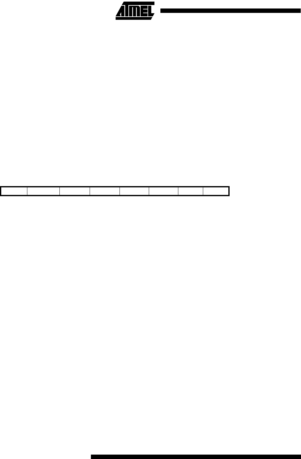
Bit 7 6 5 4 3 2 1 0
$36 ($56) OCF2 TOV2 ICF1 OCF1A OCF1B TOV1 OCF0 TOV0 TIFR
Read/Write R/W R/W R/W R/W R/W R/W R/W R/W
Initial value 0 0 0 0 0 0 0 0