
Manual


Table Of Contents
- Ordering Information
- Features
- Description
- Architectural Overview
- General Purpose Register File
- ALU - Arithmetic Logic Unit
- ISP Flash Program Memory
- SRAM Data Memory
- Program and Data Addressing Modes
- Register Direct, Single Register Rd
- Register Direct, Two Registers Rd and Rr
- I/O Direct
- Data Direct
- Data Indirect with Displacement
- Data Indirect
- Data Indirect With Pre-Decrement
- Data Indirect With Post-Increment
- Constant Addressing Using the LPM and ELPM Instructions
- Direct Program Address, JMP and CALL
- Indirect Program Addressing, IJMP and ICALL
- Relative Program Addressing, RJMP and RCALL
- EEPROM Data Memory
- Memory Access Times and Instruction Execution Timing
- I/O Memory
- Reset and Interrupt Handling
- Reset Sources
- Power-On Reset
- External Reset
- Watchdog Reset
- MCU Status Register - MCUSR
- Interrupt Handling
- External Interrupt Mask Register - EIMSK
- External Interrupt Flag Register - EIFR
- External Interrupt Control Register - EICR
- Timer/Counter Interrupt Mask Register - TIMSK
- Timer/Counter Interrupt Flag Register - TIFR
- Interrupt Response Time
- Sleep Modes
- Timer/Counters
- Timer/Counter Prescalers
- 8-bit Timer/Counters T/C0 and T/C2
- Timer/Counter0 Control Register - TCCR0
- Timer/Counter2 Control Register - TCCR2
- Timer/Counter0 - TCNT0
- Timer/Counter2 - TCNT2
- Timer/Counter0 Output Compare Register - OCR0
- Timer/Counter2 Output Compare Register - OCR2
- Timer/Counter 0 and 2 in PWM mode
- Asynchronous Status Register - ASSR
- Asynchronous Operation of Timer/Counter0
- 16-bit Timer/Counter1
- Timer/Counter1 Control Register A - TCCR1A
- Timer/Counter1 Control Register B - TCCR1B
- Timer/Counter1 - TCNT1H and TCNT1L
- Timer/Counter1 Output Compare Register - OCR1AH and OCR1AL
- Timer/Counter1 Output Compare Register - OCR1BH and OCR1BL
- Timer/Counter1 Input Capture Register - ICR1H and ICR1L
- Timer/Counter1 in PWM mode
- Watchdog Timer
- EEPROM Read/Write Access
- Serial Peripheral Interface - SPI
- UART
- Analog Comparator
- Analog to Digital Converter
- Interface to external SRAM
- I/O-Ports
- Memory Programming
- Electrical Characteristics
- Typical characteristics
- Register Summary
- Instruction Set Summary (Continued)
ATmega603/103
31
External Interrupt Control Register - EICR
•
Bits 7..0 - ISCX1, ISCX0: External Interrupt 7-4 Sense Control bits
The External Interrupts 7 - 4 are activated by the external pins INT7 - INT4 if the SREG I-flag and the corresponding inter-
rupt mask in the EIMSK is set. The level and edges on the external pins that activate the interrupts are defined in the
following table:
Note: X = 7, 6, 5 or 4.
When changing the ISCX1/ISCX0 bits, the interrupt must be disabled by clearing its Interrupt Enable bit in the GIMSK Register.
Otherwise an interrupt can occur when the bits are changed.
The value on the INTX pin is sampled before detecting edges. If edge interrupt is selected, pulses that last longer than one
CPU clock period will generate an interrupt. Shorter pulses are not guaranteed to generate an interrupt.
Observe that CPU
clock frequency can be lower than the XTAL frequency if the XTAL divider is enabled.
If low level interrupt is selected, the
low level must be held until the completion of the currently executing instruction to generate an interrupt.
If enabled, a level
triggered interrupt will generate an interrupt request as long as the pin is held low.
Timer/Counter Interrupt Mask Register - TIMSK
•
Bit 7 - OCIE2: Timer/Counter2 Output Compare Interrupt Enable
When the OCIE2 bit is set (one) and the I-bit in the Status Register is set (one), the Timer/Counter2 Compare Match inter-
rupt is enabled. The corresponding interrupt (at vector $0012) is executed if a Compare match in Timer/Counter2 occurs,
i.e., when the OCF2 bit is set in the Timer/Counter Interrupt Flag Register - TIFR.
•
Bit 6 - TOIE2: Timer/Counter2 Overflow Interrupt Enable
When the TOIE2 bit is set (one) and the I-bit in the Status Register is set (one), the Timer/Counter2 Overflow interrupt is
enabled. The corresponding interrupt (at vector $0014) is executed if an overflow in Timer/Counter2 occurs, i.e., when the
TOV2 bit is set in the Timer/Counter Interrupt Flag Register - TIFR.
•
Bit 5 - TICIE1: Timer/Counter1 Input Capture Interrupt Enable
When the TICIE1 bit is set (one) and the I-bit in the Status Register is set (one), the Timer/Counter1 Input Capture Event
Interrupt is enabled. The corresponding interrupt (at vector $0016) is executed if a capture-triggering event occurs on pin
29, PD4(IC1), i.e., when the ICF1 bit is set in the Timer/Counter Interrupt Flag Register - TIFR.
•
Bit 4 - OCE1A: Timer/Counter1 Output CompareA Match Interrupt Enable
When the OCIE1A bit is set (one) and the I-bit in the Status Register is set (one), the Timer/Counter1 CompareA Match
interrupt is enabled. The corresponding interrupt (at vector $0018) is executed if a CompareA match in Timer/Counter1
occurs, i.e., when the OCF1A bit is set in the Timer/Counter Interrupt Flag Register - TIFR.
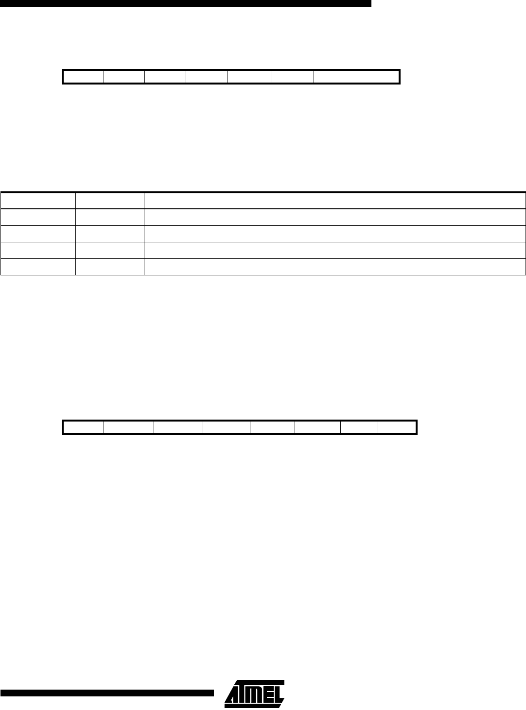
Bit 7654 3 2 1 0
$3A ($5A) ISC71 ISC70 ISC61 ISC60 ISC51 ISC50 ISC41 ISC40 EICR
Read/Write R/W R/W R/W R/W R/W R/W R/W R/W
Initial value 0 0 0 0 0 0 0 0
Table 10. Interrupt Sense Control
ISCX1 ISCX0 Description
0 0 The low level of INTX generates an interrupt request.
01Reserved
1 0 The falling edge of INTX generates an interrupt request.
1 1 The rising edge of INTX generates an interrupt request.
Bit 7 6 5 4 3 2 1 0
$37 ($57) OCIE2 TOIE2 TICIE1 OCIE1A OCIE1B TOIE1 OCIE0 TOIE0 TIMSK
Read/Write R/W R/W R/W R/W R/W R/W R/W R/W
Initial value 0 0 0 0 0 0 0 0