
Manual


Table Of Contents
- Ordering Information
- Features
- Description
- Architectural Overview
- General Purpose Register File
- ALU - Arithmetic Logic Unit
- ISP Flash Program Memory
- SRAM Data Memory
- Program and Data Addressing Modes
- Register Direct, Single Register Rd
- Register Direct, Two Registers Rd and Rr
- I/O Direct
- Data Direct
- Data Indirect with Displacement
- Data Indirect
- Data Indirect With Pre-Decrement
- Data Indirect With Post-Increment
- Constant Addressing Using the LPM and ELPM Instructions
- Direct Program Address, JMP and CALL
- Indirect Program Addressing, IJMP and ICALL
- Relative Program Addressing, RJMP and RCALL
- EEPROM Data Memory
- Memory Access Times and Instruction Execution Timing
- I/O Memory
- Reset and Interrupt Handling
- Reset Sources
- Power-On Reset
- External Reset
- Watchdog Reset
- MCU Status Register - MCUSR
- Interrupt Handling
- External Interrupt Mask Register - EIMSK
- External Interrupt Flag Register - EIFR
- External Interrupt Control Register - EICR
- Timer/Counter Interrupt Mask Register - TIMSK
- Timer/Counter Interrupt Flag Register - TIFR
- Interrupt Response Time
- Sleep Modes
- Timer/Counters
- Timer/Counter Prescalers
- 8-bit Timer/Counters T/C0 and T/C2
- Timer/Counter0 Control Register - TCCR0
- Timer/Counter2 Control Register - TCCR2
- Timer/Counter0 - TCNT0
- Timer/Counter2 - TCNT2
- Timer/Counter0 Output Compare Register - OCR0
- Timer/Counter2 Output Compare Register - OCR2
- Timer/Counter 0 and 2 in PWM mode
- Asynchronous Status Register - ASSR
- Asynchronous Operation of Timer/Counter0
- 16-bit Timer/Counter1
- Timer/Counter1 Control Register A - TCCR1A
- Timer/Counter1 Control Register B - TCCR1B
- Timer/Counter1 - TCNT1H and TCNT1L
- Timer/Counter1 Output Compare Register - OCR1AH and OCR1AL
- Timer/Counter1 Output Compare Register - OCR1BH and OCR1BL
- Timer/Counter1 Input Capture Register - ICR1H and ICR1L
- Timer/Counter1 in PWM mode
- Watchdog Timer
- EEPROM Read/Write Access
- Serial Peripheral Interface - SPI
- UART
- Analog Comparator
- Analog to Digital Converter
- Interface to external SRAM
- I/O-Ports
- Memory Programming
- Electrical Characteristics
- Typical characteristics
- Register Summary
- Instruction Set Summary (Continued)
ATmega603/103
29
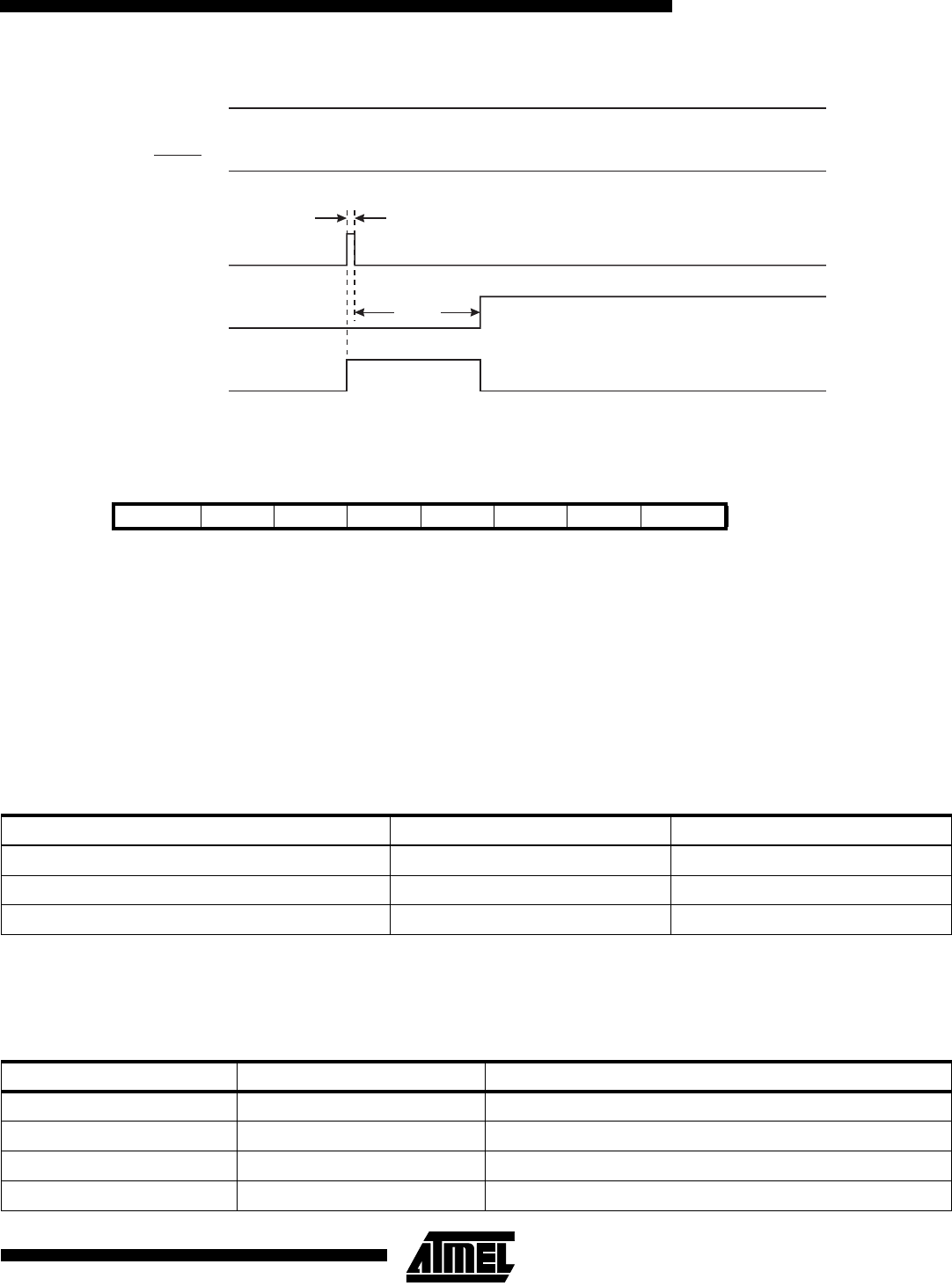
Figure 27. Watchdog Reset During Operation
MCU Status Register - MCUSR
The MCU Status Register provides information on which reset source caused an MCU reset.
•
Bits 7..2 - Res: Reserved Bits
These bits are reserved bits in the ATmega603/103 and always read as zero.
•
Bit 1 - EXTRF: External Reset Flag
After a power-on reset, this bit is undefined (X). It will be set by an external reset. A watchdog reset will leave this bit
unchanged.
•
Bit 0 - PORF: Power-on Reset Flag
This bit is set by a power-on reset. A watchdog reset or an external reset will leave this bit unchanged.
To summarize, the following table shows the value of these two bits after the three modes of reset:
To make use of these bits to identify a reset condition, the user software should clear both the PORF and EXTRF bits as
early as possible in the program. Checking the PORF and EXTRF values is done before the bits are cleared. If the bit is
cleared before an external or watchdog reset occurs, the source of reset can be found by using the following truth table:
Bit 7 654321 0
$34 ($54) - - - - - - EXTRF PORF MCUSR
Read/WriteR RRRRRR/WR/W
Initial value 0 0 0 0 0 0 See bit description
Table 8. PORF and EXTRF Values after Reset
Reset Source EXTRF PORF
Power-on Reset undefined 1
External Reset 1 unchanged
Watchdog Reset unchanged unchanged
Table 9. Reset Source Identification
EXTRF PORF Reset Source
0 0 Watchdog Reset
0 1 Power-on Reset
1 0 External Reset
1 1 Power-on Reset
VCC
RESET
RESET
TIME-OUT
INTERNAL
RESET
WDT
TIME-OUT
1 XTAL Cycle
t
TOUT