
Manual


Table Of Contents
- Ordering Information
- Features
- Description
- Architectural Overview
- General Purpose Register File
- ALU - Arithmetic Logic Unit
- ISP Flash Program Memory
- SRAM Data Memory
- Program and Data Addressing Modes
- Register Direct, Single Register Rd
- Register Direct, Two Registers Rd and Rr
- I/O Direct
- Data Direct
- Data Indirect with Displacement
- Data Indirect
- Data Indirect With Pre-Decrement
- Data Indirect With Post-Increment
- Constant Addressing Using the LPM and ELPM Instructions
- Direct Program Address, JMP and CALL
- Indirect Program Addressing, IJMP and ICALL
- Relative Program Addressing, RJMP and RCALL
- EEPROM Data Memory
- Memory Access Times and Instruction Execution Timing
- I/O Memory
- Reset and Interrupt Handling
- Reset Sources
- Power-On Reset
- External Reset
- Watchdog Reset
- MCU Status Register - MCUSR
- Interrupt Handling
- External Interrupt Mask Register - EIMSK
- External Interrupt Flag Register - EIFR
- External Interrupt Control Register - EICR
- Timer/Counter Interrupt Mask Register - TIMSK
- Timer/Counter Interrupt Flag Register - TIFR
- Interrupt Response Time
- Sleep Modes
- Timer/Counters
- Timer/Counter Prescalers
- 8-bit Timer/Counters T/C0 and T/C2
- Timer/Counter0 Control Register - TCCR0
- Timer/Counter2 Control Register - TCCR2
- Timer/Counter0 - TCNT0
- Timer/Counter2 - TCNT2
- Timer/Counter0 Output Compare Register - OCR0
- Timer/Counter2 Output Compare Register - OCR2
- Timer/Counter 0 and 2 in PWM mode
- Asynchronous Status Register - ASSR
- Asynchronous Operation of Timer/Counter0
- 16-bit Timer/Counter1
- Timer/Counter1 Control Register A - TCCR1A
- Timer/Counter1 Control Register B - TCCR1B
- Timer/Counter1 - TCNT1H and TCNT1L
- Timer/Counter1 Output Compare Register - OCR1AH and OCR1AL
- Timer/Counter1 Output Compare Register - OCR1BH and OCR1BL
- Timer/Counter1 Input Capture Register - ICR1H and ICR1L
- Timer/Counter1 in PWM mode
- Watchdog Timer
- EEPROM Read/Write Access
- Serial Peripheral Interface - SPI
- UART
- Analog Comparator
- Analog to Digital Converter
- Interface to external SRAM
- I/O-Ports
- Memory Programming
- Electrical Characteristics
- Typical characteristics
- Register Summary
- Instruction Set Summary (Continued)
ATmega603/103
27
Power-On Reset
A Power-On Reset (POR) circuit ensures that the device is reset from power-on. As shown in Figure 23, an internal timer
clocked from the Watchdog timer oscillator prevents the MCU from starting until after a certain period after V
CC
has
reached the Power-On Threshold voltage - V
POT
, regardless of the V
CC
rise time (see Figure 24). The Fuse bits SUT1 and
SUT0 is used to select start-up time as indicated in Table 6. A “0” in the table indicates that the fuse is programmed.
The user can select the start-up time according to typical oscillator start-up time. The number of WDT oscillator cycles used
for each time-out except for SUT = 00 is shown in Table 7. The frequency of the watchdog oscillator is voltage dependent
as shown in “Typical characteristics” on page 110.
The setting SUT 1/0 = 00 starts the MCU after 5 CPU clock cycles, and can be used when an external clock signal is
applied to the XTAL1 pin. This setting does not use the WDT oscillator, and enables very fast start-up from the sleep
modes power down or power save if the clock signal is present during sleep. For details, refer to the programming specifi-
cation starting on page 92.
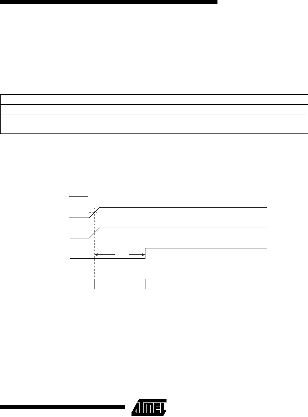
If the built-in start-up delay is sufficient, RESET
can be connected to V
CC
directly or via an external pull-up resistor. By hold-
ing the pin low for a period after V
CC
has been applied, the Power-On Reset period can be extended. Refer to Figure 25 for
a timing example on this.
Figure 24. MCU Start-Up, RESET
Tied to V
CC
.
Table 7. Number of watchdog oscillator cycles
SUT 1/0 Time-out at V
CC
= 5V Number of WDT cycles
01 0.5 ms 512
10 4.0 ms 4K
11 16.0 ms 16K
VCC
RESET
TIME-OUT
INTERNAL
RESET
t
TOUT
V
POT
V
RST