
Manual


Table Of Contents
- Ordering Information
- Features
- Description
- Architectural Overview
- General Purpose Register File
- ALU - Arithmetic Logic Unit
- ISP Flash Program Memory
- SRAM Data Memory
- Program and Data Addressing Modes
- Register Direct, Single Register Rd
- Register Direct, Two Registers Rd and Rr
- I/O Direct
- Data Direct
- Data Indirect with Displacement
- Data Indirect
- Data Indirect With Pre-Decrement
- Data Indirect With Post-Increment
- Constant Addressing Using the LPM and ELPM Instructions
- Direct Program Address, JMP and CALL
- Indirect Program Addressing, IJMP and ICALL
- Relative Program Addressing, RJMP and RCALL
- EEPROM Data Memory
- Memory Access Times and Instruction Execution Timing
- I/O Memory
- Reset and Interrupt Handling
- Reset Sources
- Power-On Reset
- External Reset
- Watchdog Reset
- MCU Status Register - MCUSR
- Interrupt Handling
- External Interrupt Mask Register - EIMSK
- External Interrupt Flag Register - EIFR
- External Interrupt Control Register - EICR
- Timer/Counter Interrupt Mask Register - TIMSK
- Timer/Counter Interrupt Flag Register - TIFR
- Interrupt Response Time
- Sleep Modes
- Timer/Counters
- Timer/Counter Prescalers
- 8-bit Timer/Counters T/C0 and T/C2
- Timer/Counter0 Control Register - TCCR0
- Timer/Counter2 Control Register - TCCR2
- Timer/Counter0 - TCNT0
- Timer/Counter2 - TCNT2
- Timer/Counter0 Output Compare Register - OCR0
- Timer/Counter2 Output Compare Register - OCR2
- Timer/Counter 0 and 2 in PWM mode
- Asynchronous Status Register - ASSR
- Asynchronous Operation of Timer/Counter0
- 16-bit Timer/Counter1
- Timer/Counter1 Control Register A - TCCR1A
- Timer/Counter1 Control Register B - TCCR1B
- Timer/Counter1 - TCNT1H and TCNT1L
- Timer/Counter1 Output Compare Register - OCR1AH and OCR1AL
- Timer/Counter1 Output Compare Register - OCR1BH and OCR1BL
- Timer/Counter1 Input Capture Register - ICR1H and ICR1L
- Timer/Counter1 in PWM mode
- Watchdog Timer
- EEPROM Read/Write Access
- Serial Peripheral Interface - SPI
- UART
- Analog Comparator
- Analog to Digital Converter
- Interface to external SRAM
- I/O-Ports
- Memory Programming
- Electrical Characteristics
- Typical characteristics
- Register Summary
- Instruction Set Summary (Continued)
ATmega603/103
23
•
Bits 4,3 - SM1/SM0: Sleep Mode Select bits 1 and 0
This bit selects between the three available sleep modes as shown in the following table:
•
Bits 2..0 - Res: Reserved bits
These bits are reserved bits in the ATmega603/103 and always read zero.
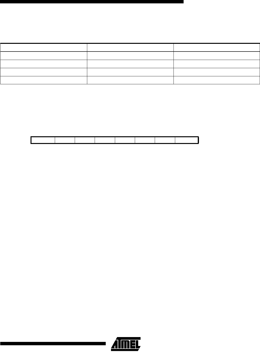
XTAL Divide Control Register - XDIV
The XTAL Divide Control Register is used to divide the XTAL clock frequency by a number in the range 1 - 129. This fea-
ture can be used to decrease power consumption when the requirement for processing power is low.
•
Bit 7 - XDIVEN: XTAL Divide Enable
When the XDIVEN bit is set (one), the clock frequency of the CPU and all peripherals is divided by the factor defined by the
setting of XDIV6 - XDIV0. This bit can be set and cleared run-time to vary the clock frequency as suitable to the application.
•
Bits 6..0 - XDIV6..XDIV0: XTAL Divide Select Bits 6 - 0
These bits define the division factor that applies when the XDIVEN bit is set (one). If the value of these bits is denoted
d
,
the following formula defines the resulting CPU clock frequency
f
clk
:
The value of these bits can only be changed when XDIVEN is zero. When XDIVEN is set to one, the value written simulta-
neously into XDIV6..XDIV0 is taken as the division factor. When XDIVEN is cleared to zero, the value written
simultaneously into XDIV6..XDIV0 is rejected. As the divider divides the master clock input to the MCU, the speed of all
peripherals is reduced when a division factor is used.
Table 4. Sleep Mode Select
SM1 SM0 Sleep Mode
0 0 Idle Mode
01Reserved
1 0 Power Down
1 1 Power Save
Bit 7 654321 0
$3C ($5C) XDIVEN XDIV6 XDIV5 XDIV4 XDIV3 XDIV2 XDIV1 XDIV0 XDIV
Read/Write R/W R/W R/W R/W R/W R/W R/W R/W
Initial value0 000000 0
f
CLK
XTAL
129 d–
-------------------=