
Manual


Table Of Contents
- Ordering Information
- Features
- Description
- Architectural Overview
- General Purpose Register File
- ALU - Arithmetic Logic Unit
- ISP Flash Program Memory
- SRAM Data Memory
- Program and Data Addressing Modes
- Register Direct, Single Register Rd
- Register Direct, Two Registers Rd and Rr
- I/O Direct
- Data Direct
- Data Indirect with Displacement
- Data Indirect
- Data Indirect With Pre-Decrement
- Data Indirect With Post-Increment
- Constant Addressing Using the LPM and ELPM Instructions
- Direct Program Address, JMP and CALL
- Indirect Program Addressing, IJMP and ICALL
- Relative Program Addressing, RJMP and RCALL
- EEPROM Data Memory
- Memory Access Times and Instruction Execution Timing
- I/O Memory
- Reset and Interrupt Handling
- Reset Sources
- Power-On Reset
- External Reset
- Watchdog Reset
- MCU Status Register - MCUSR
- Interrupt Handling
- External Interrupt Mask Register - EIMSK
- External Interrupt Flag Register - EIFR
- External Interrupt Control Register - EICR
- Timer/Counter Interrupt Mask Register - TIMSK
- Timer/Counter Interrupt Flag Register - TIFR
- Interrupt Response Time
- Sleep Modes
- Timer/Counters
- Timer/Counter Prescalers
- 8-bit Timer/Counters T/C0 and T/C2
- Timer/Counter0 Control Register - TCCR0
- Timer/Counter2 Control Register - TCCR2
- Timer/Counter0 - TCNT0
- Timer/Counter2 - TCNT2
- Timer/Counter0 Output Compare Register - OCR0
- Timer/Counter2 Output Compare Register - OCR2
- Timer/Counter 0 and 2 in PWM mode
- Asynchronous Status Register - ASSR
- Asynchronous Operation of Timer/Counter0
- 16-bit Timer/Counter1
- Timer/Counter1 Control Register A - TCCR1A
- Timer/Counter1 Control Register B - TCCR1B
- Timer/Counter1 - TCNT1H and TCNT1L
- Timer/Counter1 Output Compare Register - OCR1AH and OCR1AL
- Timer/Counter1 Output Compare Register - OCR1BH and OCR1BL
- Timer/Counter1 Input Capture Register - ICR1H and ICR1L
- Timer/Counter1 in PWM mode
- Watchdog Timer
- EEPROM Read/Write Access
- Serial Peripheral Interface - SPI
- UART
- Analog Comparator
- Analog to Digital Converter
- Interface to external SRAM
- I/O-Ports
- Memory Programming
- Electrical Characteristics
- Typical characteristics
- Register Summary
- Instruction Set Summary (Continued)
ATmega603/103
21
The different I/O and peripherals control registers are explained in the following sections.
Status Register - SREG
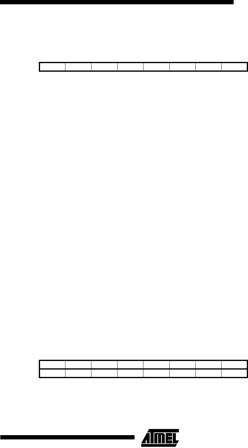
The AVR status register - SREG - at I/O space location $3F ($5F) is defined as:
•
Bit 7 - I: Global Interrupt Enable
The global interrupt enable bit must be set (one) for the interrupts to be enabled. The individual interrupt enable control is
then performed in separate control registers. If the global interrupt enable register is cleared (zero), none of the interrupts
are enabled independent of the individual interrupt enable settings. The I-bit is cleared by hardware after an interrupt has
occurred, and is set by the RETI instruction to enable subsequent interrupts.
•
Bit 6 - T: Bit Copy Storage
The bit copy instructions BLD (Bit LoaD) and BST (Bit STore) use the T bit as source and destination for the operated bit. A
bit from a register in the register file can be copied into T by the BST instruction, and a bit in T can be copied into a bit in a
register in the register file by the BLD instruction.
•
Bit 5 - H: Half Carry Flag
The half carry flag H indicates a half carry in some arithmetic operations. See the Instruction Set Description for detailed
information.
•
Bit 4 - S: Sign Bit, S = N ⊕ V
The S-bit is always an exclusive or between the negative flag N and the two’s complement overflow flag V. See the Instruc-
tion Set Description for detailed information.
•
Bit 3 - V: Two’s Complement Overflow Flag
The two’s complement overflow flag V supports two’s complement arithmetics. See the Instruction Set Description for
detailed information.
•
Bit 2 - N: Negative Flag
The negative flag N indicates a negative result from an arithmetical or logical operation. See the Instruction Set Description
for detailed information.
•
Bit 1 - Z: Zero Flag
The zero flag Z indicates a zero result from an arithmetical or logical operation. See the Instruction Set Description for
detailed information.
•
Bit 0 - C: Carry Flag
The carry flag C indicates a carry in an arithmetical or logical operation. See the Instruction Set Description for detailed
information.
Note that the status register is not automatically stored when entering an interrupt routine and restored when returning from
an interrupt routine. This must be handled by software.
Stack Pointer - SP
The general AVR 16-bit Stack Pointer is effectively built up of two 8-bit registers in the I/O space locations $3E ($5E) and
$3D ($5D). As the ATmega603/103 supports up to 64 kB memory, all 16-bits are used.
Bit 76543210
$3F ($5F) I T H S V N Z C SREG
Read/Write R/W R/W R/W R/W R/W R/W R/W R/W
Initial value00000000
Bit 151413121110 9 8
$3E ($5E) SP15 SP14 SP13 SP12 SP11 SP10 SP9 SP8 SPH
$3D ($5D) SP7 SP6 SP5 SP4 SP3 SP2 SP1 SP0 SPL
76543210
Read/Write R/W R/W R/W R/W R/W R/W R/W R/W
R/W R/W R/W R/W R/W R/W R/W R/W
Initial value00000000
00000000