
Manual


Table Of Contents
- Ordering Information
- Features
- Description
- Architectural Overview
- General Purpose Register File
- ALU - Arithmetic Logic Unit
- ISP Flash Program Memory
- SRAM Data Memory
- Program and Data Addressing Modes
- Register Direct, Single Register Rd
- Register Direct, Two Registers Rd and Rr
- I/O Direct
- Data Direct
- Data Indirect with Displacement
- Data Indirect
- Data Indirect With Pre-Decrement
- Data Indirect With Post-Increment
- Constant Addressing Using the LPM and ELPM Instructions
- Direct Program Address, JMP and CALL
- Indirect Program Addressing, IJMP and ICALL
- Relative Program Addressing, RJMP and RCALL
- EEPROM Data Memory
- Memory Access Times and Instruction Execution Timing
- I/O Memory
- Reset and Interrupt Handling
- Reset Sources
- Power-On Reset
- External Reset
- Watchdog Reset
- MCU Status Register - MCUSR
- Interrupt Handling
- External Interrupt Mask Register - EIMSK
- External Interrupt Flag Register - EIFR
- External Interrupt Control Register - EICR
- Timer/Counter Interrupt Mask Register - TIMSK
- Timer/Counter Interrupt Flag Register - TIFR
- Interrupt Response Time
- Sleep Modes
- Timer/Counters
- Timer/Counter Prescalers
- 8-bit Timer/Counters T/C0 and T/C2
- Timer/Counter0 Control Register - TCCR0
- Timer/Counter2 Control Register - TCCR2
- Timer/Counter0 - TCNT0
- Timer/Counter2 - TCNT2
- Timer/Counter0 Output Compare Register - OCR0
- Timer/Counter2 Output Compare Register - OCR2
- Timer/Counter 0 and 2 in PWM mode
- Asynchronous Status Register - ASSR
- Asynchronous Operation of Timer/Counter0
- 16-bit Timer/Counter1
- Timer/Counter1 Control Register A - TCCR1A
- Timer/Counter1 Control Register B - TCCR1B
- Timer/Counter1 - TCNT1H and TCNT1L
- Timer/Counter1 Output Compare Register - OCR1AH and OCR1AL
- Timer/Counter1 Output Compare Register - OCR1BH and OCR1BL
- Timer/Counter1 Input Capture Register - ICR1H and ICR1L
- Timer/Counter1 in PWM mode
- Watchdog Timer
- EEPROM Read/Write Access
- Serial Peripheral Interface - SPI
- UART
- Analog Comparator
- Analog to Digital Converter
- Interface to external SRAM
- I/O-Ports
- Memory Programming
- Electrical Characteristics
- Typical characteristics
- Register Summary
- Instruction Set Summary (Continued)
ATmega603/103
19
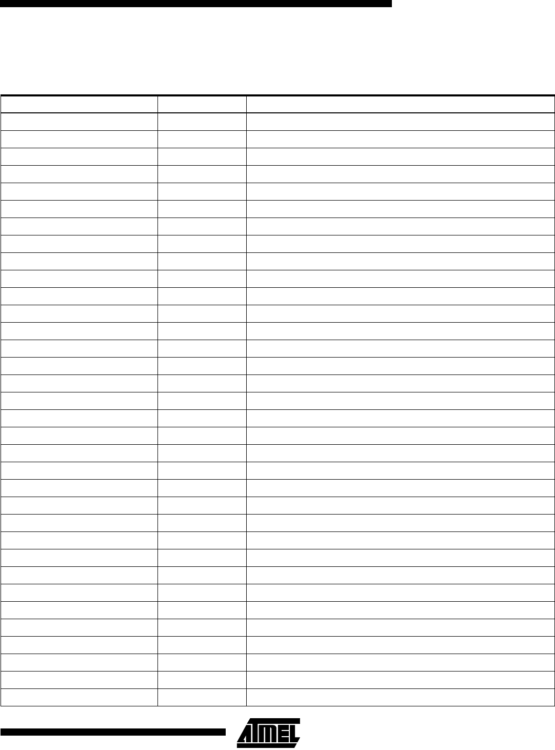
I/O Memory
The I/O space definition of the ATmega603/103 is shown in the following table:
Table 3. ATmega603/103 I/O Space
I/O Address (SRAM Address) Name Function
$3F ($5F) SREG Status REGister
$3E ($5E) SPH Stack Pointer High
$3D ($5D) SPL Stack Pointer Low
$3C ($5C) XDIV XTAL Divide Control Register
$3B ($5B) RAMPZ RAM Page Z Select Register
$3A ($5A) EICR External Interrupt Control Register
$39 ($59) EIMSK External Interrupt MaSK register
$38 ($58) EIFR External Interrupt Flag Register
$37 ($57) TIMSK Timer/Counter Interrupt MaSK register
$36 ($56) TIFR Timer/Counter Interrupt Flag register
$35 ($55) MCUCR MCU General Control Register
$34 ($54) MCUSR MCU Status Register
$33 ($53) TCCR0 Timer/Counter0 Control Register
$32 ($52) TCNT0 Timer/Counter0 (8-bit)
$31 ($51) OCR0 Timer/Counter0 Output Compare Register
$30 ($50) ASSR Asynchronous Mode Status Register
$2F ($4F) TCCR1A Timer/Counter1 Control Register A
$2E ($4E) TCCR1B Timer/Counter1 Control Register B
$2D ($4D) TCNT1H Timer/Counter1 High Byte
$2C ($4C) TCNT1L Timer/Counter1 Low Byte
$2B ($4B) OCR1AH Timer/Counter1 Output Compare Register A High Byte
$2A ($4A) OCR1AL Timer/Counter1 Output Compare Register A Low Byte
$29 ($49) OCR1BH Timer/Counter1 Output Compare Register B High Byte
$28 ($48) OCR1BL Timer/Counter1 Output Compare Register B Low Byte
$27 ($47) ICR1H Timer/Counter1 Input Capture Register High Byte
$26 ($46) ICR1L Timer/Counter1 Input Capture Register Low Byte
$25 ($45) TCCR2 Timer/Counter2 Control Register
$24 ($44) TCNT2 Timer/Counter2 (8-bit)
$23 ($43) OCR2 Timer/Counter2 Output Compare Register
$21 ($41) WDTCR Watchdog Timer Control Register
$1F ($3F) EEARH EEPROM Address Register High
$1E ($3E) EEARL EERPOM Address Register Low
$1D ($3D) EEDR EEPROM Data Register
$1C ($3C) EECR EEPROM Control Register