
Manual


Table Of Contents
- Ordering Information
- Features
- Description
- Architectural Overview
- General Purpose Register File
- ALU - Arithmetic Logic Unit
- ISP Flash Program Memory
- SRAM Data Memory
- Program and Data Addressing Modes
- Register Direct, Single Register Rd
- Register Direct, Two Registers Rd and Rr
- I/O Direct
- Data Direct
- Data Indirect with Displacement
- Data Indirect
- Data Indirect With Pre-Decrement
- Data Indirect With Post-Increment
- Constant Addressing Using the LPM and ELPM Instructions
- Direct Program Address, JMP and CALL
- Indirect Program Addressing, IJMP and ICALL
- Relative Program Addressing, RJMP and RCALL
- EEPROM Data Memory
- Memory Access Times and Instruction Execution Timing
- I/O Memory
- Reset and Interrupt Handling
- Reset Sources
- Power-On Reset
- External Reset
- Watchdog Reset
- MCU Status Register - MCUSR
- Interrupt Handling
- External Interrupt Mask Register - EIMSK
- External Interrupt Flag Register - EIFR
- External Interrupt Control Register - EICR
- Timer/Counter Interrupt Mask Register - TIMSK
- Timer/Counter Interrupt Flag Register - TIFR
- Interrupt Response Time
- Sleep Modes
- Timer/Counters
- Timer/Counter Prescalers
- 8-bit Timer/Counters T/C0 and T/C2
- Timer/Counter0 Control Register - TCCR0
- Timer/Counter2 Control Register - TCCR2
- Timer/Counter0 - TCNT0
- Timer/Counter2 - TCNT2
- Timer/Counter0 Output Compare Register - OCR0
- Timer/Counter2 Output Compare Register - OCR2
- Timer/Counter 0 and 2 in PWM mode
- Asynchronous Status Register - ASSR
- Asynchronous Operation of Timer/Counter0
- 16-bit Timer/Counter1
- Timer/Counter1 Control Register A - TCCR1A
- Timer/Counter1 Control Register B - TCCR1B
- Timer/Counter1 - TCNT1H and TCNT1L
- Timer/Counter1 Output Compare Register - OCR1AH and OCR1AL
- Timer/Counter1 Output Compare Register - OCR1BH and OCR1BL
- Timer/Counter1 Input Capture Register - ICR1H and ICR1L
- Timer/Counter1 in PWM mode
- Watchdog Timer
- EEPROM Read/Write Access
- Serial Peripheral Interface - SPI
- UART
- Analog Comparator
- Analog to Digital Converter
- Interface to external SRAM
- I/O-Ports
- Memory Programming
- Electrical Characteristics
- Typical characteristics
- Register Summary
- Instruction Set Summary (Continued)
ATmega603/103
110
Typical characteristics
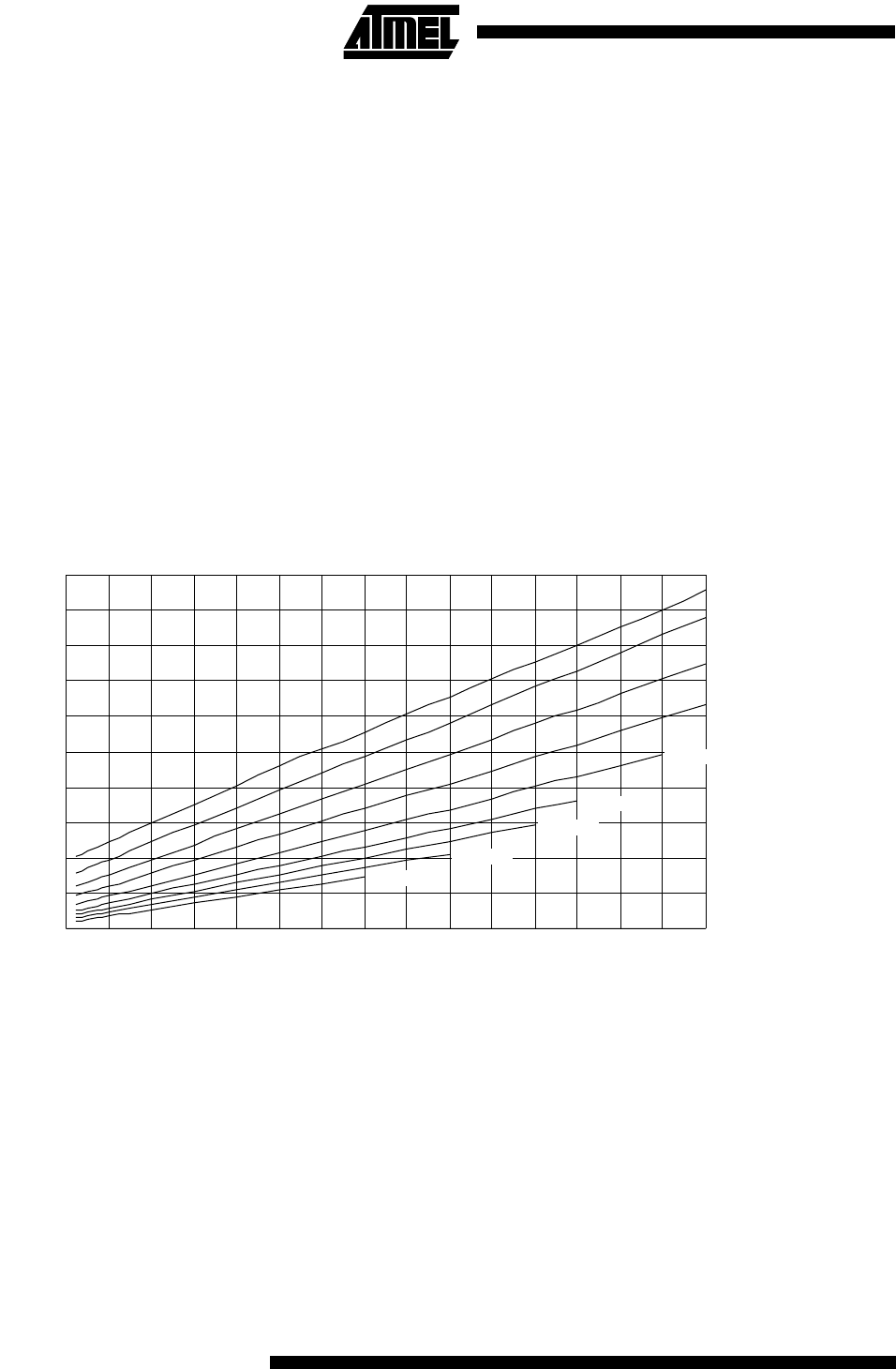
The following charts show typical behavior. These data are characterized, but not tested. All current consumption measure-
ments are performed with all I/O pins configured as inputs and with internal pull-ups enabled. All pins on Port F pulled high
externally. A sine wave generator with rail to rail output is used as clock source.
The power consumption in power-down mode is independent of clock selection.
The current consumption is a function of several factors such as: operating voltage, operating frequency, loading of I/O
pins, switching rate of I/O pins, code executed and ambient temperature. The dominating factors are operating voltage and
frequency.
The current drawn from capacitive loaded pins may be estimated (for one pin) as C
L
*V
CC
*f where C
L
= load capacitance,
V
CC
= operating voltage and f = average switching frequency of I/O pin.
The parts are characterized at frequencies higher than test limits. Parts are not guaranteed to function properly at frequen-
cies higher than the ordering code indicates.
The difference between current consumption in Power Down mode with Watchdog timer enabled and Power Down mode
with Watchdog timer disabled represents the differential current drawn by the watchdog timer.
Figure 80. Active Supply Current vs. Frequency
0
5
10
15
20
25
30
35
40
45
50
0 1 2 3 4 5 6 7 8 9 10 11 12 13 14 15
ACTIVE SUPPLY CURRENT vs. FREQUENCY
T = 25˚C
A
Frequency (MHz)
I
cc
(mA)
V
cc
= 5.5V
V
cc
= 5V
V
cc
= 2.7V
V
cc
= 3.0V
V
cc
= 3.3V
V
cc
= 3.6V
V
cc
= 4V
V
cc
= 4.5V
V
cc
= 6V