
Manual


Table Of Contents
- Ordering Information
- Features
- Description
- Architectural Overview
- General Purpose Register File
- ALU - Arithmetic Logic Unit
- ISP Flash Program Memory
- SRAM Data Memory
- Program and Data Addressing Modes
- Register Direct, Single Register Rd
- Register Direct, Two Registers Rd and Rr
- I/O Direct
- Data Direct
- Data Indirect with Displacement
- Data Indirect
- Data Indirect With Pre-Decrement
- Data Indirect With Post-Increment
- Constant Addressing Using the LPM and ELPM Instructions
- Direct Program Address, JMP and CALL
- Indirect Program Addressing, IJMP and ICALL
- Relative Program Addressing, RJMP and RCALL
- EEPROM Data Memory
- Memory Access Times and Instruction Execution Timing
- I/O Memory
- Reset and Interrupt Handling
- Reset Sources
- Power-On Reset
- External Reset
- Watchdog Reset
- MCU Status Register - MCUSR
- Interrupt Handling
- External Interrupt Mask Register - EIMSK
- External Interrupt Flag Register - EIFR
- External Interrupt Control Register - EICR
- Timer/Counter Interrupt Mask Register - TIMSK
- Timer/Counter Interrupt Flag Register - TIFR
- Interrupt Response Time
- Sleep Modes
- Timer/Counters
- Timer/Counter Prescalers
- 8-bit Timer/Counters T/C0 and T/C2
- Timer/Counter0 Control Register - TCCR0
- Timer/Counter2 Control Register - TCCR2
- Timer/Counter0 - TCNT0
- Timer/Counter2 - TCNT2
- Timer/Counter0 Output Compare Register - OCR0
- Timer/Counter2 Output Compare Register - OCR2
- Timer/Counter 0 and 2 in PWM mode
- Asynchronous Status Register - ASSR
- Asynchronous Operation of Timer/Counter0
- 16-bit Timer/Counter1
- Timer/Counter1 Control Register A - TCCR1A
- Timer/Counter1 Control Register B - TCCR1B
- Timer/Counter1 - TCNT1H and TCNT1L
- Timer/Counter1 Output Compare Register - OCR1AH and OCR1AL
- Timer/Counter1 Output Compare Register - OCR1BH and OCR1BL
- Timer/Counter1 Input Capture Register - ICR1H and ICR1L
- Timer/Counter1 in PWM mode
- Watchdog Timer
- EEPROM Read/Write Access
- Serial Peripheral Interface - SPI
- UART
- Analog Comparator
- Analog to Digital Converter
- Interface to external SRAM
- I/O-Ports
- Memory Programming
- Electrical Characteristics
- Typical characteristics
- Register Summary
- Instruction Set Summary (Continued)
ATmega603/103
109
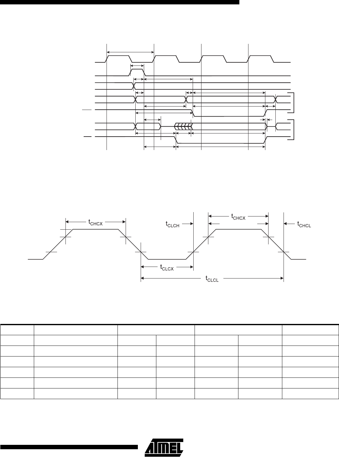
Figure 78. External RAM Timing
External Clock Drive Waveforms
Figure 79. External Clock Drive Waveforms
Table 50. External Clock Drive
Note: See “External Data Memory Timing” on page 107 for a description of how the duty cycle influences the timing for the External
Data Memory
Symbol Parameter V
CC
= 2.7V to 3.6V V
CC
= 4.0V to 5.5V Units
1/t
CLCL
Oscillator Frequency 0 4 0 6 MHz
t
CLCL
Clock Period 250 167 ns
t
CHCX
High Time 100 67 ns
t
CLCX
Low Time 100 67 ns
t
CLCH
Rise Time 1.6 0.5 µs
t
CHCL
Fall Time 1.6 0.5 µs
System Clock O
ALE
WR
RD
Data / Address [7..0]
Data / Address [7..0]
Address [15..8]
Address
Address
Address
T1 T2 T3 T4
Prev. Address
Prev. Address
Prev. Address
1
0
4
213
3a
5
Note: Clock cycle T3 is only present when external SRAM waitstate is enabled
10
12
14
15
11
8
9
16
7
6
3b
Data
Data
WriteRead
Addr.
Addr.
VIL1
VIH1