
Manual
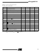


Table Of Contents
- Ordering Information
- Features
- Description
- Architectural Overview
- General Purpose Register File
- ALU - Arithmetic Logic Unit
- ISP Flash Program Memory
- SRAM Data Memory
- Program and Data Addressing Modes
- Register Direct, Single Register Rd
- Register Direct, Two Registers Rd and Rr
- I/O Direct
- Data Direct
- Data Indirect with Displacement
- Data Indirect
- Data Indirect With Pre-Decrement
- Data Indirect With Post-Increment
- Constant Addressing Using the LPM and ELPM Instructions
- Direct Program Address, JMP and CALL
- Indirect Program Addressing, IJMP and ICALL
- Relative Program Addressing, RJMP and RCALL
- EEPROM Data Memory
- Memory Access Times and Instruction Execution Timing
- I/O Memory
- Reset and Interrupt Handling
- Reset Sources
- Power-On Reset
- External Reset
- Watchdog Reset
- MCU Status Register - MCUSR
- Interrupt Handling
- External Interrupt Mask Register - EIMSK
- External Interrupt Flag Register - EIFR
- External Interrupt Control Register - EICR
- Timer/Counter Interrupt Mask Register - TIMSK
- Timer/Counter Interrupt Flag Register - TIFR
- Interrupt Response Time
- Sleep Modes
- Timer/Counters
- Timer/Counter Prescalers
- 8-bit Timer/Counters T/C0 and T/C2
- Timer/Counter0 Control Register - TCCR0
- Timer/Counter2 Control Register - TCCR2
- Timer/Counter0 - TCNT0
- Timer/Counter2 - TCNT2
- Timer/Counter0 Output Compare Register - OCR0
- Timer/Counter2 Output Compare Register - OCR2
- Timer/Counter 0 and 2 in PWM mode
- Asynchronous Status Register - ASSR
- Asynchronous Operation of Timer/Counter0
- 16-bit Timer/Counter1
- Timer/Counter1 Control Register A - TCCR1A
- Timer/Counter1 Control Register B - TCCR1B
- Timer/Counter1 - TCNT1H and TCNT1L
- Timer/Counter1 Output Compare Register - OCR1AH and OCR1AL
- Timer/Counter1 Output Compare Register - OCR1BH and OCR1BL
- Timer/Counter1 Input Capture Register - ICR1H and ICR1L
- Timer/Counter1 in PWM mode
- Watchdog Timer
- EEPROM Read/Write Access
- Serial Peripheral Interface - SPI
- UART
- Analog Comparator
- Analog to Digital Converter
- Interface to external SRAM
- I/O-Ports
- Memory Programming
- Electrical Characteristics
- Typical characteristics
- Register Summary
- Instruction Set Summary (Continued)
ATmega603/103
108
Notes: 1. This assumes 50% clock duty cycle. The half period is actually the high time of the external clock, XTAL1.
2. This assumes 50% clock duty cycle. The half period is actually the low time of the external clock, XTAL1.
Table 48. External Data Memory Characteristics, 2.7 - 3.6 Volts, No Wait State
Symbol Parameter
4 MHz Oscillator Variable Oscillator
UnitMin Max Min Max
01/t
CLCL
Oscillator Frequency 0.0 4.0 MHz
1t
LHLL
ALE Pulse Width 65.0 0.5t
CLCL
-60.0
(1)
ns
2t
AVLL
Address Valid A to ALE Low 75.0 0.5t
CLCL
-50.0
(1)
ns
3a t
LLAX_ST
Address Hold After ALE Low,
ST/STD/STS Instructions
125.0 0.5t
CLCL
(2)
ns
3b t
LLAX_LD
Address Hold after ALE Low,
LD/LDD/LDS Instructions
15.0 15.0
ns
4t
AVLLC
Address Valid C to ALE Low 75.0 0.5t
CLCL
-50.0
(1)
ns
5t
AVRL
Address Valid to RD Low 205.0 1.0t
CLCL
-45.0 ns
6t
AVWL
Address Valid to WR Low 325.0 1.5t
CLCL
-50.0
(1)
ns
7t
LLWL
ALE Low to WR Low 230.0 270.0 1.0t
CLCL
-20.0 1.0t
CLCL
+20.0 ns
8t
LLRL
ALE Low to RD Low 105.0 145.0 0.5t
CLCL
-20.0
(2)
0.5t
CLCL
+20.0
(2)
ns
9t
DVRH
Data Setup to RD High 110.0 110.0 ns
10 t
RLDV
Read Low to Data Valid 210.0 1.0t
CLCL
-40.0 ns
11 t
RHDX
Data Hold After RD High 0.0 0.0 ns
12 t
RLRH
RD Pulse Width 230.0 1.0t
CLCL
-20.0 ns
13 t
DVWL
Data Setup to WR Low 90.0 0.5t
CLCL
-35.0
(1)
ns
14 t
WHDX
Data Hold After WR High 0.0 0.0 ns
15 t
DVWH
Data Valid to WR High 230.0 1.0t
CLCL
-20.0 ns
16 t
WLWH
WR Pulse Width 100.0 0.5t
CLCL
-25.0
(2)
ns
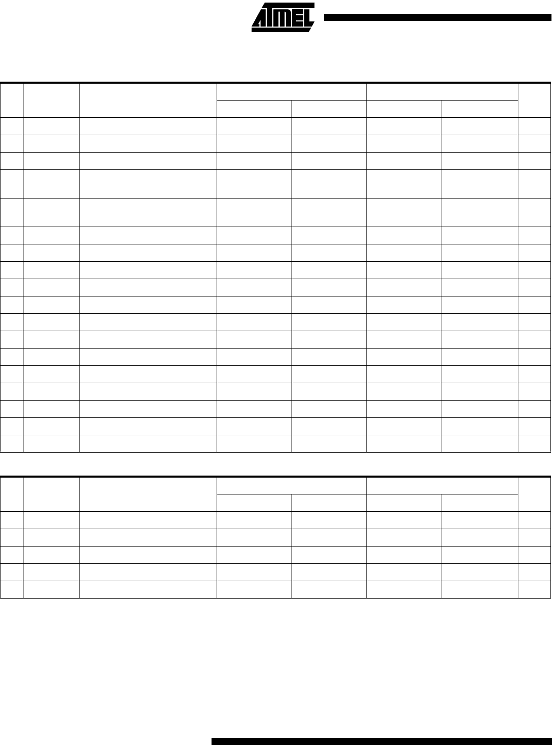
Table 49. External Data Memory Characteristics, 2.7 -3.6 Volts, 1 Cycle Wait State
Symbol Parameter
4 MHz Oscillator Variable Oscillator
UnitMin Max Min Max
01/t
CLCL
Oscillator Frequency 0.0 4.0 MHz
10 t
RLDV
Read Low to Data Valid 460.00 2.0t
CLCL
-40.0 ns
12 t
RLRH
RD Pulse Width 480.0 2.0t
CLCL
-20.0 ns
15 t
DVWH
Data Valid to WR High 480.0 2.0t
CLCL
-20.0 ns
16 t
WLWH
WR Pulse Width 350.0 1.5t
CLCL
-25.0
(2)
ns