
Manual
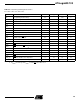


Table Of Contents
- Ordering Information
- Features
- Description
- Architectural Overview
- General Purpose Register File
- ALU - Arithmetic Logic Unit
- ISP Flash Program Memory
- SRAM Data Memory
- Program and Data Addressing Modes
- Register Direct, Single Register Rd
- Register Direct, Two Registers Rd and Rr
- I/O Direct
- Data Direct
- Data Indirect with Displacement
- Data Indirect
- Data Indirect With Pre-Decrement
- Data Indirect With Post-Increment
- Constant Addressing Using the LPM and ELPM Instructions
- Direct Program Address, JMP and CALL
- Indirect Program Addressing, IJMP and ICALL
- Relative Program Addressing, RJMP and RCALL
- EEPROM Data Memory
- Memory Access Times and Instruction Execution Timing
- I/O Memory
- Reset and Interrupt Handling
- Reset Sources
- Power-On Reset
- External Reset
- Watchdog Reset
- MCU Status Register - MCUSR
- Interrupt Handling
- External Interrupt Mask Register - EIMSK
- External Interrupt Flag Register - EIFR
- External Interrupt Control Register - EICR
- Timer/Counter Interrupt Mask Register - TIMSK
- Timer/Counter Interrupt Flag Register - TIFR
- Interrupt Response Time
- Sleep Modes
- Timer/Counters
- Timer/Counter Prescalers
- 8-bit Timer/Counters T/C0 and T/C2
- Timer/Counter0 Control Register - TCCR0
- Timer/Counter2 Control Register - TCCR2
- Timer/Counter0 - TCNT0
- Timer/Counter2 - TCNT2
- Timer/Counter0 Output Compare Register - OCR0
- Timer/Counter2 Output Compare Register - OCR2
- Timer/Counter 0 and 2 in PWM mode
- Asynchronous Status Register - ASSR
- Asynchronous Operation of Timer/Counter0
- 16-bit Timer/Counter1
- Timer/Counter1 Control Register A - TCCR1A
- Timer/Counter1 Control Register B - TCCR1B
- Timer/Counter1 - TCNT1H and TCNT1L
- Timer/Counter1 Output Compare Register - OCR1AH and OCR1AL
- Timer/Counter1 Output Compare Register - OCR1BH and OCR1BL
- Timer/Counter1 Input Capture Register - ICR1H and ICR1L
- Timer/Counter1 in PWM mode
- Watchdog Timer
- EEPROM Read/Write Access
- Serial Peripheral Interface - SPI
- UART
- Analog Comparator
- Analog to Digital Converter
- Interface to external SRAM
- I/O-Ports
- Memory Programming
- Electrical Characteristics
- Typical characteristics
- Register Summary
- Instruction Set Summary (Continued)
ATmega603/103
106
Notes: 1. “Max” means the highest value where the pin is guaranteed to be read as low
2. “Min” means the lowest value where the pin is guaranteed to be read as high
3. Although each I/O port can sink more than the test conditions (20mA at Vcc = 5V, 10mA at Vcc = 3V) under steady state
conditions ( non-transient), the following must be observed:
1] The sum of all IOL, for all ports, should not exceed 400 mA.
2] The sum of all IOL, for ports A0-A7, ALE, C3-C7 should not exceed 100 mA.
3] The sum of all IOL, for ports C0-C2, RD
, WR, D0-D7, XTAL2 should not exceed 100 mA.
4] The sum of all IOL, for ports B0-B7, should not exceed 100 mA.
5] The sum of all IOL, for ports E0-E7, should not exceed 100 mA.
If IOL exceeds the test condition, VOL may exceed the related specification. Pins are not guaranteed to sink current greater
than the listed test condition.
4. Although each I/O port can source more than the test conditions (3mA at Vcc = 5V, 1.5mA at Vcc = 3V) under steady state
conditions ( non-transient), the following must be observed:
1] The sum of all IOH, for all ports, should not exceed 400 mA.
2] The sum of all IOH, for ports A0-A7, ALE, C3-C7 should not exceed 100 mA.
3] The sum of all IOH, for ports C0-C2, RD
, WR, D0-D7, XTAL2 should not exceed 100 mA.
4] The sum of all IOH, for ports B0-B7, should not exceed 100 mA.
5] The sum of all IOH, for ports E0-E7, should not exceed 100 mA.
If IOH exceeds the test condition, VOH may exceed the related specification. Pins are not guaranteed to source current
greater than the listed test condition.
5. Minimum V
CC
for Power Down is 2V.
RRST Reset Pullup 100 500 kΩ
R
I/O
I/O Pin Pullup 35 120 kΩ
I
CC
Power Supply Current Active 4 MHz, V
CC
= 3V 5.0 mA
Idle 4 MHz, V
CC
= 3V 2.0 mA
Power Down
(5)
, V
CC
= 3V
WDT Enabled
40.0 µA
Power Down
(5)
, V
CC
= 3V
WDT Disabled
25.0 µA
Power Save
(5)
, V
CC
= 3V
WDT Disabled
35.0 µA
V
ACIO
Analog Comp
Input Offset V
V
CC
= 5V 40 mV
I
ACLK
Analog Comp
Input Leakage A
V
CC
= 5V
V
IN
= V
CC
/2
-50 50 nA
t
ACPD
Analog Comparator
Propagation Delay
V
CC
= 2.7V
V
CC
= 4.0V
750
500
ns
DC Characteristics (Continued)
T
A
= -40°C to 85°C V
CC
= 2.7V to 3.6V and 4.0V to 5.5V (unless otherwise noted) (Continued)
Symbol Parameter Condition Min Typ Max Units