
Manual


Table Of Contents
- Ordering Information
- Features
- Description
- Architectural Overview
- General Purpose Register File
- ALU - Arithmetic Logic Unit
- ISP Flash Program Memory
- SRAM Data Memory
- Program and Data Addressing Modes
- Register Direct, Single Register Rd
- Register Direct, Two Registers Rd and Rr
- I/O Direct
- Data Direct
- Data Indirect with Displacement
- Data Indirect
- Data Indirect With Pre-Decrement
- Data Indirect With Post-Increment
- Constant Addressing Using the LPM and ELPM Instructions
- Direct Program Address, JMP and CALL
- Indirect Program Addressing, IJMP and ICALL
- Relative Program Addressing, RJMP and RCALL
- EEPROM Data Memory
- Memory Access Times and Instruction Execution Timing
- I/O Memory
- Reset and Interrupt Handling
- Reset Sources
- Power-On Reset
- External Reset
- Watchdog Reset
- MCU Status Register - MCUSR
- Interrupt Handling
- External Interrupt Mask Register - EIMSK
- External Interrupt Flag Register - EIFR
- External Interrupt Control Register - EICR
- Timer/Counter Interrupt Mask Register - TIMSK
- Timer/Counter Interrupt Flag Register - TIFR
- Interrupt Response Time
- Sleep Modes
- Timer/Counters
- Timer/Counter Prescalers
- 8-bit Timer/Counters T/C0 and T/C2
- Timer/Counter0 Control Register - TCCR0
- Timer/Counter2 Control Register - TCCR2
- Timer/Counter0 - TCNT0
- Timer/Counter2 - TCNT2
- Timer/Counter0 Output Compare Register - OCR0
- Timer/Counter2 Output Compare Register - OCR2
- Timer/Counter 0 and 2 in PWM mode
- Asynchronous Status Register - ASSR
- Asynchronous Operation of Timer/Counter0
- 16-bit Timer/Counter1
- Timer/Counter1 Control Register A - TCCR1A
- Timer/Counter1 Control Register B - TCCR1B
- Timer/Counter1 - TCNT1H and TCNT1L
- Timer/Counter1 Output Compare Register - OCR1AH and OCR1AL
- Timer/Counter1 Output Compare Register - OCR1BH and OCR1BL
- Timer/Counter1 Input Capture Register - ICR1H and ICR1L
- Timer/Counter1 in PWM mode
- Watchdog Timer
- EEPROM Read/Write Access
- Serial Peripheral Interface - SPI
- UART
- Analog Comparator
- Analog to Digital Converter
- Interface to external SRAM
- I/O-Ports
- Memory Programming
- Electrical Characteristics
- Typical characteristics
- Register Summary
- Instruction Set Summary (Continued)
ATmega603/103
105
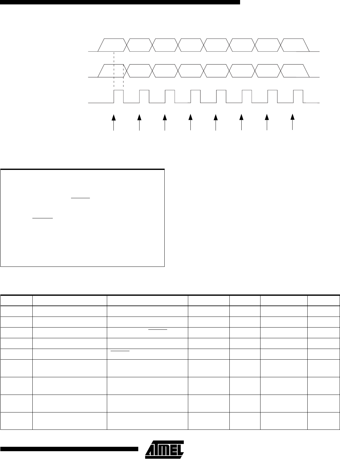
Figure 77. Serial Programming Waveforms
Electrical Characteristics
Absolute Maximum Ratings*
Operating Temperature.................................. -40°C to +105°C
*NOTICE: Stresses beyond those listed under “Absolute
Maximum Ratings” may cause permanent dam-
age to the device. This is a stress rating only and
functional operation of the device at these or
other conditions beyond those indicated in the
operational sections of this specification is not
implied. Exposure to absolute maximum rating
conditions for extended periods may affect device
reliability.
Storage Temperature..................................... -65°C to +150°C
Voltage on any Pin except RESET
with respect to Ground ................................-1.0V to V
CC
+0.5V
Voltage on RESET
with respect to Ground......-1.0V to +13.0V
Maximum Operating Voltage ............................................ 6.6V
DC Current per I/O Pin ............................................... 40.0 mA
DC Current
V
CC
and GND........................................ 400.0 mA
DC Characteristics
T
A
= -40°C to 85°C V
CC
= 2.7V to 3.6V and 4.0V to 5.5V (unless otherwise noted)
Symbol Parameter Condition Min Typ Max Units
V
IL
Input Low Voltage Except (XTAL) -0.5 0.3 V
CC
(1)
V
V
IL1
Input Low Voltage XTAL -0.5 0.1
(1)
V
V
IH
Input High Voltage Except (XTAL, RESET) 0.6 V
CC
(2)
V
CC
+ 0.5 V
V
IH1
Input High Voltage XTAL 0.7 V
CC
(2)
V
CC
+ 0.5 V
V
IH2
Input High Voltage RESET 0.85 V
CC
(2)
V
CC
+ 0.5 V
V
OL
Output Low Voltage
(3)
Ports A, B, C, D, E
I
OL
= 20 mA, V
CC
= 5V
I
OL
= 10 mA, V
CC
= 3V
0.6
0.5
V
V
V
OH
Output High Voltage
(4)
Ports A, B, C, D, E
I
OH
= -3 mA, V
CC
= 5V
I
OH
= -1.5 mA, V
CC
= 3V
4.3
2.2
V
V
I
IL
Input Leakage
Current I/O Pin
V
CC
= 6V, Pin Low
(Absolute value)
8.0 µ
A
I
IH
Input Leakage
Current I/O Pin
V
CC
= 6V, Pin High
(Absolute value)
8.0 µA
MSB
MSB
LSB
LSB
SERIAL CLOCK INPUT
PB1(SCK)
SERIAL DATA INPUT
PE0(PDI/RXD)
SERIAL DATA OUTPUT
PE1(PDO/TXD)
SAMPLE