
Manual
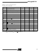


Table Of Contents
- Ordering Information
- Features
- Description
- Architectural Overview
- General Purpose Register File
- ALU - Arithmetic Logic Unit
- ISP Flash Program Memory
- SRAM Data Memory
- Program and Data Addressing Modes
- Register Direct, Single Register Rd
- Register Direct, Two Registers Rd and Rr
- I/O Direct
- Data Direct
- Data Indirect with Displacement
- Data Indirect
- Data Indirect With Pre-Decrement
- Data Indirect With Post-Increment
- Constant Addressing Using the LPM and ELPM Instructions
- Direct Program Address, JMP and CALL
- Indirect Program Addressing, IJMP and ICALL
- Relative Program Addressing, RJMP and RCALL
- EEPROM Data Memory
- Memory Access Times and Instruction Execution Timing
- I/O Memory
- Reset and Interrupt Handling
- Reset Sources
- Power-On Reset
- External Reset
- Watchdog Reset
- MCU Status Register - MCUSR
- Interrupt Handling
- External Interrupt Mask Register - EIMSK
- External Interrupt Flag Register - EIFR
- External Interrupt Control Register - EICR
- Timer/Counter Interrupt Mask Register - TIMSK
- Timer/Counter Interrupt Flag Register - TIFR
- Interrupt Response Time
- Sleep Modes
- Timer/Counters
- Timer/Counter Prescalers
- 8-bit Timer/Counters T/C0 and T/C2
- Timer/Counter0 Control Register - TCCR0
- Timer/Counter2 Control Register - TCCR2
- Timer/Counter0 - TCNT0
- Timer/Counter2 - TCNT2
- Timer/Counter0 Output Compare Register - OCR0
- Timer/Counter2 Output Compare Register - OCR2
- Timer/Counter 0 and 2 in PWM mode
- Asynchronous Status Register - ASSR
- Asynchronous Operation of Timer/Counter0
- 16-bit Timer/Counter1
- Timer/Counter1 Control Register A - TCCR1A
- Timer/Counter1 Control Register B - TCCR1B
- Timer/Counter1 - TCNT1H and TCNT1L
- Timer/Counter1 Output Compare Register - OCR1AH and OCR1AL
- Timer/Counter1 Output Compare Register - OCR1BH and OCR1BL
- Timer/Counter1 Input Capture Register - ICR1H and ICR1L
- Timer/Counter1 in PWM mode
- Watchdog Timer
- EEPROM Read/Write Access
- Serial Peripheral Interface - SPI
- UART
- Analog Comparator
- Analog to Digital Converter
- Interface to external SRAM
- I/O-Ports
- Memory Programming
- Electrical Characteristics
- Typical characteristics
- Register Summary
- Instruction Set Summary (Continued)

ATmega603/103
104
Note: a = address high bits
b = address low bits
H = 0 - Low byte, 1 - High byte
o = data out
i = data in
x = don’t care
1
= Lock Bit 1
2
= Lock Bit 2
3 = SUT0 Fuse
4 = SUT1 Fuse
5 = SPIEN Fuse
6 = EESAVE Fuse
Table 45. Serial Programming Instruction Set
Instruction Instruction Format Operation
Byte 1 Byte 2 Byte 3 Byte 4
Programming Enable
1010 1100 0101 0011 xxxx xxxx xxxx xxxx Enable Serial Programming while
RESET
is low.
Chip Erase 1010 1100 100x xxxx xxxx xxxx xxxx xxxx Chip Erase EEPROM and Flash.
Read Program Memory
0010 H000 aaaa aaaa bbbb bbbb oooo oooo Read H(high or low) data o from
Program memory at word address
a:b.
Load Program Memory
Page
0100 H000 xxxx xxxx xbbb bbbb iiii iiii Write H (high or low) data i to
Program page memory at word
address b.
Write Program Memory
Page
0100 1100 aaaa aaaa bxxx xxxx xxxx xxxx Write Program Memory Page at
address a:b.
Read EEPROM Memory
1010 0000 xxxx aaaa bbbb bbbb oooo oooo Read data o from EEPROM
memory at address a:b.
Write EEPROM Memory
1100 0000 xxxx aaaa bbbb bbbb iiii iiii Write data i to EEPROM memory
at address a:b.
Read Lock Bits
0101 1000 xxxx xxxx xxxx xxxx xxxx x
21
x Read Lock bits. ‘0’ = programmed,
‘1’ = unprogrammed.
Write Lock Bits
1010 1100 1111 1
21
1 xxxx xxxx xxxx xxxx Write Lock bits. Set bits
1,2
= ’0’ to
program Lock bits.
Read Fuse Bits
0101 0000 xxxx xxxx xxxx xxxx xx5x 6143 Read Fuse bits. ‘0’ = programmed,
‘1’ = unprogrammed.
Write Fuse Bits
1010 1100 1011 6143 xxxx xxxx xxxx xxxx Write Fuse bits. Set bit 6,4
,
3
= ’0’
to program, ‘1’ to unprogram.
Read Signature Byte
0011 0000 xxxx xxxx xxxx xxbb oooo oooo Read Signature Byte o at address
b.