
Manual


Table Of Contents
- Ordering Information
- Features
- Description
- Architectural Overview
- General Purpose Register File
- ALU - Arithmetic Logic Unit
- ISP Flash Program Memory
- SRAM Data Memory
- Program and Data Addressing Modes
- Register Direct, Single Register Rd
- Register Direct, Two Registers Rd and Rr
- I/O Direct
- Data Direct
- Data Indirect with Displacement
- Data Indirect
- Data Indirect With Pre-Decrement
- Data Indirect With Post-Increment
- Constant Addressing Using the LPM and ELPM Instructions
- Direct Program Address, JMP and CALL
- Indirect Program Addressing, IJMP and ICALL
- Relative Program Addressing, RJMP and RCALL
- EEPROM Data Memory
- Memory Access Times and Instruction Execution Timing
- I/O Memory
- Reset and Interrupt Handling
- Reset Sources
- Power-On Reset
- External Reset
- Watchdog Reset
- MCU Status Register - MCUSR
- Interrupt Handling
- External Interrupt Mask Register - EIMSK
- External Interrupt Flag Register - EIFR
- External Interrupt Control Register - EICR
- Timer/Counter Interrupt Mask Register - TIMSK
- Timer/Counter Interrupt Flag Register - TIFR
- Interrupt Response Time
- Sleep Modes
- Timer/Counters
- Timer/Counter Prescalers
- 8-bit Timer/Counters T/C0 and T/C2
- Timer/Counter0 Control Register - TCCR0
- Timer/Counter2 Control Register - TCCR2
- Timer/Counter0 - TCNT0
- Timer/Counter2 - TCNT2
- Timer/Counter0 Output Compare Register - OCR0
- Timer/Counter2 Output Compare Register - OCR2
- Timer/Counter 0 and 2 in PWM mode
- Asynchronous Status Register - ASSR
- Asynchronous Operation of Timer/Counter0
- 16-bit Timer/Counter1
- Timer/Counter1 Control Register A - TCCR1A
- Timer/Counter1 Control Register B - TCCR1B
- Timer/Counter1 - TCNT1H and TCNT1L
- Timer/Counter1 Output Compare Register - OCR1AH and OCR1AL
- Timer/Counter1 Output Compare Register - OCR1BH and OCR1BL
- Timer/Counter1 Input Capture Register - ICR1H and ICR1L
- Timer/Counter1 in PWM mode
- Watchdog Timer
- EEPROM Read/Write Access
- Serial Peripheral Interface - SPI
- UART
- Analog Comparator
- Analog to Digital Converter
- Interface to external SRAM
- I/O-Ports
- Memory Programming
- Electrical Characteristics
- Typical characteristics
- Register Summary
- Instruction Set Summary (Continued)
ATmega603/103
101
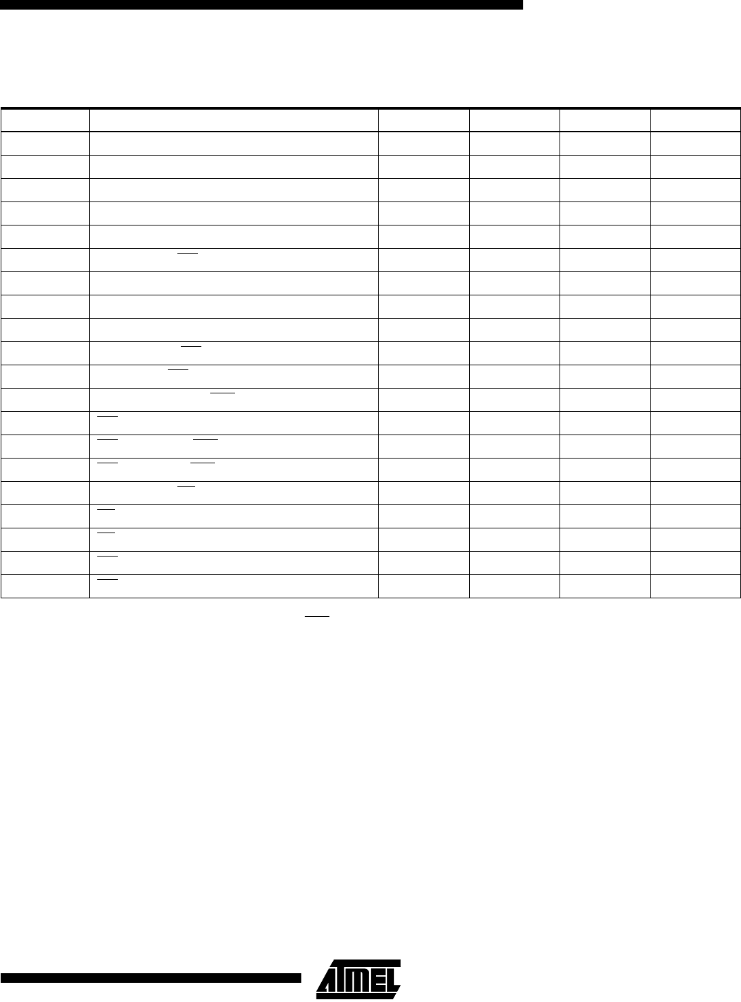
Table 42. Parallel Programming Characteristics
T
A
= 25
°
C ± 10%, V
CC
=5V ± 10%
Notes: 1. Use t
WLWH_CE
for Chip Erase and t
WLWH_PFB
for Programming the Fuse Bits.
2. If t
WLWH
is held longer than t
WLRH
, no RDY/BSY pulse will be seen.
Symbol Parameter Min Typ Max Units
V
PP
Programming Enable Voltage 11.5 12.5 V
I
PP
Programming Enable Current 250 µA
t
DVXH
Data and Control Valid before XTAL1 High 67 ns
t
XHXL
XTAL1 Pulse Width High 67 ns
t
XLDX
Data and Control Hold after XTAL1 Low 67 ns
t
XLWL
XTAL1 Low to WR Low 67 ns
t
BVXH
BS1 Valid before XTAL1 High 67 ns
t
PHPL
PAGEL Pulse Width High 67 ns
t
PLBX
BS1 Hold after PAGEL Low 67 ns
t
PLWL
PAGEL Low to WR Low 67 ns
t
BVWL
BS1 Valid to WR Low 67 ns
t
RHBX
BS1 Hold after RDY/BSY High 67 ns
t
WLWH
WR Pulse Width Low
(1)
67 ns
t
WHRL
WR High to RDY/BSY Low
(2)
20 ns
t
WLRH
WR Low to RDY/BSY High
(2)
0.5 0.7 0.9 ms
t
XLOL
XTAL1 Low to OE Low 67 ns
t
OLDV
OE Low to DATA Valid 20 ns
t
OHDZ
OE High to DATA Tri-stated 20 ns
t
WLWH_CE
WR Pulse Width Low for Chip Erase 5 10 15 ms
t
WLWH_PFB
WR Pulse Width Low for Progr. the Fuse Bits 1.0 1.5 1.8 ms