
Manual

3
ATAR862-8
4589B–4BMCU–02/03
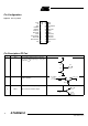
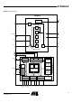
5 XTAL Connection for crystal
6 VS Supply voltage ESD protection circuitry (see Figure 8)
7 GND Ground ESD protection circuitry (see Figure 8)
8 ENABLE Enable input
Pin Description: RF Part (Continued)
Pin Symbol Function Configuration
XTAL
1.2k
VS
1.5k
VS
182 mA
ENABLE
200k
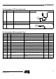
Pin Description: Microcontroller Part
Name Type Function Alternate Function Pin-No.
Reset State
V
DD
– Supply voltage – 13
NA
V
SS
– Circuit ground – 12
NA
BP20 I/O Bi-directional I/O line of Port 2.0 NTE-test mode enable, see also section "Master Reset" 7
Input
BP40 I/O Bi-directional I/O line of Port 4.0 SC-serial clock or INT3 external interrupt input 14
Input
BP41 I/O Bi-directional I/O line of Port 4.1
VMI voltage monitor input or T2I external clock input
Timer 2
9
Input
BP42 I/O Bi-directional I/O line of Port 4.2 T2O Timer 2 output 10
Input
BP43 I/O Bi-directional I/O line of Port 4.3 SD serial data I/O or INT3-external interrupt input 11
Input
BP50 I/O Bi-directional I/O line of Port 5.0 INT6 external interrupt input 17
Input
BP52 I/O Bi-directional I/O line of Port 5.2 INT1 external interrupt input 16
Input
BP53 I/O Bi-directional I/O line of Port 5.3 INT1 external interrupt input 15
Input
BP60 I/O Bi-directional I/O line of Port 6.0 T3O Timer 3 output 20
Input
BP63 I/O Bi-directional I/O line of Port 6.3 T3I Timer 3 input 6
Input
OSC1 I Oscillator input
4-MHz crystal input or 32-kHz crystal input or external
clock input or external trimming resistor input
18
Input
OSC2 O Oscillator output
4-MHz crystal output or 32-kHz crystal output or external
clock input
19
Input
NRESET I/O Bi-directional reset pin – 5
I/O