
Manual

11
ATAR862-8
4589B–4BMCU–02/03
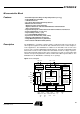
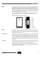
Figure 8. ESD Protection Circuit
CLK PA_ENABLE
ANT2
ANT1
XTAL ENABLE
VS
GND
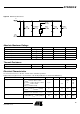
Absolute Maximum Ratings
Parameters Symbol Min. Max. Unit
Supply voltage V
S
5V
Power dissipation P
tot
100 mW
Junction temperature T
j
150 °C
Storage temperature T
Stg
-55 +125 °C
Ambient temperature T
amb
-55 +125 °C
Thermal Resistance
Parameters Symbol Value Unit
Junction ambient R
thJA
170 K/W
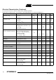
Electrical Characteristics
V
S
= 2.0 V to 4.0 V, T
amb
= -40°C to +125°C unless otherwise specified.
Typical values are given at V
S
= 3.0 V and T
amb
= 25°C. All parameters are referred to GND (Pin 7).
Parameters Test Conditions Symbol Min. Typ. Max. Unit
Supply current Power down,
V
ENABLE
< 0.25 V, -40°C to +85°C
V
PA_ENABLE
< 0.25 V, -85°C to +125°C
V
PA_ENABLE
< 0.25 V, +25°C
(100% correlation tested)
I
S_Off
<10
350
7
nA
µA
nA
Supply current Power up, PA off, V
S
= 3 V
V
ENABLE
> 1.7 V, V
PA - E N AB L E
<0.25V
I
S
3.7 4.8 mA
Power up, V
S
= 3.0 V
V
ENABLE
> 1.7 V, V
PA - E N AB L E
>1.7V
I
S_Transmit
8.5 11 mA
Output power V
S
= 3.0 V, T
amb
=25°C
f = 868.3 MHz, Z
Load
= (166 + j226) W
P
Ref
3.5 5.5 8 dBm