
Manual


8
4912C–AUTO–10/06
ATA6827 [Preliminary]
7. Noise and Surge Immunity
Parameters Test Conditions Value
Conducted interferences ISO 7637-1 Level 4
(1)
Interference suppression VDE 0879 Part 2 Level 5
ESD (Human Body Model) ESD S 5.1 2 kV
CDM (Charged Device Model) ESD STM 5.3.1-1999 all pins 500V
Note: Test pulse 5: V
smax
= 40V
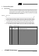
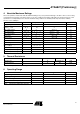
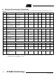
8. Electrical Characteristics
7.5V < V
VS
< 40V; 4.75V < V
VCC
< 5.25 V; INH = High; –40°C ≤ T
j
≤ 200°C; T
a
≤ 150°C; unless otherwise specified, all values refer to
GND pins.
No. Parameters Test Conditions Pin Symbol Min. Typ. Max. Unit Type*
1 Current Consumption
1.1 Quiescent current VS V
VS
< 20V, INH = low 10, 11 I
VS
1 60 µA A
1.2 Quiescent current VCC
4.75 V < V
VCC
< 5.25V,
INH = low
9 I
VCC
15 40 µA A
1.3 Supply current VS
V
VS
< 20V normal
operating, all outputs off
10, 11 I
VS
4 6 mA A
1.4 Supply current VCC
4.75V < V
VCC
< 5.25V,
normal operating
9 I
VCC
350 500 µA A
1.5 Discharge current VS
V
VS
= 32.5V,
INH = low
10, 11 I
VS
0.5 5.5 mA A
1.6 Discharge current VS
V
VS
= 40V,
INH = low
10, 11 I
VS
2.0 10 mA A
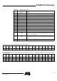
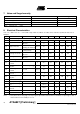
2 Undervoltage Detection, Power-on Reset
2.1
Power-on reset
threshold
9 V
VCC
3.1 3.9 4.5 V A
2.2
Power-on reset
delay time
After switching on V
CC
t
dPor
30 95 190 µs A
2.3
Undervoltage-detection
threshold
V
CC
= 5V 10, 11 V
Uv
5.5 7.1 V A
2.4
Undervoltage-detection
hysteresis
V
CC
= 5V 10, 11 ∆V
Uv
0.6 V A
2.5
Undervoltage-detection
delay time
t
dUV
10 40 µs A
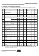
3 Thermal Prewarning and Shutdown
3.1 Thermal prewarning set T
jPW set
170 195 220 °C B
3.2
Thermal prewarning
reset
T
jPW reset
155 180 205 °C B
3.3
Thermal prewarning
hysteresis
∆T
jPW
15 °C B
3.4 Thermal shutdown off T
j switch off
200 225 250 °C B
3.5 Thermal shutdown on T
j switch on
185 210 235 °C B
*) Type means: A =100% tested, B = 100% correlation tested, C = Characterized on samples, D = Design parameter
Note: 1. Delay time between rising edge of the input signal at pin CS after data transmission and switch on output stages to 90% of
final level. Device not in standby for t > 1 ms