
Manual


4
4912C–AUTO–10/06
ATA6827 [Preliminary]
3. Functional Description
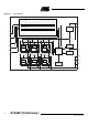
3.1 Serial Interface
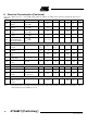
Data transfer starts with the falling edge of the CS signal. Data must appear at DI synchronized
to CLK and are accepted on the falling edge of the CLK signal. LSB (bit 0, SRR) has to be trans-
ferred first. Execution of new input data is enabled on the rising edge of the CS signal. When CS
is high, pin DO is in tri-state condition. This output is enabled on the falling edge of CS. Output
data will change their state with the rising edge of CLK and stay stable until the next rising edge
of CLK appears. LSB (bit 0, TP) is transferred first.
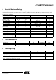
Figure 3-1. Data Transfer
SRR LS1 HS1 LS2 HS2 LS3
HS3
n. u.
n. u. n. u. n. u. n. u. n. u.
OCS
n. u. n. u.
CS
DI
CLK
DO
TP S1L S1H S2L S2H S3L S3H n. u.
n. u. n. u. n. u. n. u. n. u. SCD OPL PSF
0 1 2 3 4 5 6 7 8 9 10 11 12 13 14 15
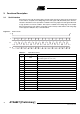
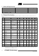
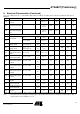
Table 3-1. Input Data Protocol
Bit Input Register Function
0SRR
Status register reset (high = reset; the bits PSF, OPL and SCD in the
output data register are set to low)
1
LS1 Controls output LS1 (high = switch output LS1 on)
2
HS1 Controls output HS1 (high = switch output HS1 on)
3
LS2 See LS1
4
HS2 See HS1
5
LS3 See LS1
6
HS3 See HS1
7
n. u. Not used
8
n. u. Not used
9
n. u. Not used
10
n. u. Not used
11
n. u. Not used
12
n. u. Not used
13
OCS Overcurrent shutdown (high = overcurrent shutdown is active)
14
n. u. Not used
15
n. u. Not used